ZHCSFG1B January   2016  – February 2017 SN75LVPE802

PRODUCTION DATA.  

  1. 特性
  2. 应用
  3. 说明
  4. 修订历史记录
  5. 说明 (续)
  6. Pin Configuration and Functions
  7. Specifications
    1. 7.1 Absolute Maximum Ratings
    2. 7.2 ESD Ratings
    3. 7.3 Recommended Operating Conditions
    4. 7.4 Thermal Information
    5. 7.5 Electrical Characteristics
    6. 7.6 Timing Requirements
    7. 7.7 Switching Characteristics
    8. 7.8 Typical Characteristics
      1. 7.8.1 Jitter and VOD results: Case 1 at 6 Gbps
      2. 7.8.2 Jitter and VOD Results: Case 2 at 3 Gbps
      3. 7.8.3 Jitter and VOD Results: Case 3 at 1.5 Gbps
      4. 7.8.4 Jitter and VOD Results: Case 4 at 8 Gbps
  8. Detailed Description
    1. 8.1 Overview
    2. 8.2 Functional Block Diagram
    3. 8.3 Feature Description
      1. 8.3.1  SATA Express
      2. 8.3.2  Receiver Termination
      3. 8.3.3  Receiver Internal Bias
      4. 8.3.4  Input Equalization
      5. 8.3.5  OOB/Squelch
      6. 8.3.6  Auto Low Power
      7. 8.3.7  Transmitter Output Signal
      8. 8.3.8  Transmitter Common Mode
      9. 8.3.9  De-Emphasis
      10. 8.3.10 Transmitter Termination
    4. 8.4 Device Functional Modes
      1. 8.4.1 Low-Power Mode
  9. Application and Implementation
    1. 9.1 Application Information
    2. 9.2 Typical SATA Application
      1. 9.2.1 Design Requirements
      2. 9.2.2 Detailed Design Procedure
        1. 9.2.2.1 Equalization Configuration
      3. 9.2.3 De-emphasis Configuration
      4. 9.2.4 Application Curves
        1. 9.2.4.1 SN75LVPE802 Equalization Settings for Various Input Trace Length
        2. 9.2.4.2 SN75LVCP802 De-emphasis Settings For various Output Trace Lengths
    3. 9.3 SATA Express Applications
      1. 9.3.1 Detailed Design Procedure
      2. 9.3.2 PCIe Applications
  10. 10Power Supply Recommendations
  11. 11Layout
    1. 11.1 Layout Guidelines
    2. 11.2 Layout Example
  12. 12器件和文档支持
    1. 12.1 接收文档更新通知
    2. 12.2 社区资源
    3. 12.3 商标
    4. 12.4 静电放电警告
    5. 12.5 Glossary
  13. 13机械、封装和可订购信息

封装选项

请参考 PDF 数据表获取器件具体的封装图。

机械数据 (封装 | 引脚)
  • RTJ|20
散热焊盘机械数据 (封装 | 引脚)
订购信息

Layout

Layout Guidelines

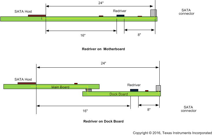
SN75LVPE802 Trace_Length_example_for_LVPE802.gif
Trace lengths are suggested values based on TI spice simulations (done over programmable limits of input EQ and output de-emphasis) to meet SATA loss and jitter spec.
Actual trace length supported by the LVPE802 may be more or less than suggested values and will depend on board layout, trace widths and number of connectors used in the SATA signal path.
Figure 46. Trace Length Example for LVPE802

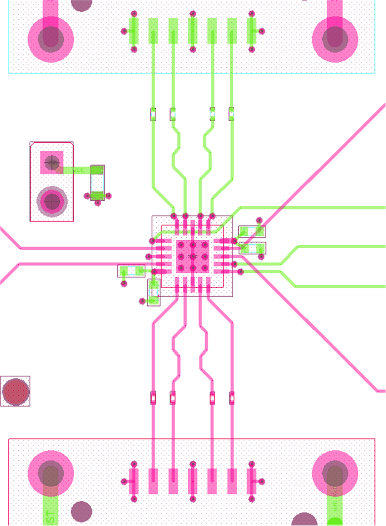
Layout Example

SN75LVPE802 Layout_Example.gif Figure 47. Example Layout