SLRS023E December 1976 – January 2015 SN75468 , SN75469
PRODUCTION DATA.
- 1 Features
- 2 Applications
- 3 Description
- 4 Simplified Schematic
- 5 Revision History
- 6 Pin Configuration and Functions
- 7 Specifications
- 8 Parameter Measurement Information
- 9 Detailed Description
- 10Application and Implementation
- 11Power Supply Recommendations
- 12Layout
- 13Device and Documentation Support
- 14Mechanical, Packaging, and Orderable Information
封装选项
请参考 PDF 数据表获取器件具体的封装图。
机械数据 (封装 | 引脚)
- NS|16
- N|16
- D|16
散热焊盘机械数据 (封装 | 引脚)
订购信息
6 Pin Configuration and Functions
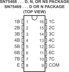
Pin Functions
| PIN | TYPE | DESCRIPTION | |
|---|---|---|---|
| NAME | NO. | ||
| <1:7>B | 1 - 7 | I | Channel 1 through 7 darlington base input |
| <1:7>C | 16 - 10 | O | Channel 1 through 7 darlington collector output |
| E | 7 | — | Common Emmitter shared by all channels (typically tied to ground) |
| COM | 8 | I/O | Common cathode node for flyback diodes (required for inductive loads) |