SCAS581N November 1996 – November 2014 SN74LVCR2245A
PRODUCTION DATA.
- 1 Features
- 2 Applications
- 3 Description
- 4 Simplified Schematic
- 5 Revision History
- 6 Pin Configuration and Functions
- 7 Specifications
- 8 Parameter Measurement Information
- 9 Detailed Description
- 10Application and Implementation
- 11Power Supply Recommendations
- 12Layout
- 13Device and Documentation Support
封装选项
请参考 PDF 数据表获取器件具体的封装图。
机械数据 (封装 | 引脚)
- DGV|20
- DB|20
- DBQ|20
- NS|20
- PW|20
- DW|20
- RGY|20
散热焊盘机械数据 (封装 | 引脚)
订购信息
6 Pin Configuration and Functions
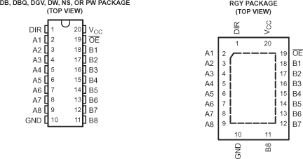
Pin Functions
| PIN | TYPE | DESCRIPTION | |
|---|---|---|---|
| NO. | NAME | ||
| 1 | DIR | I | Direction Pin |
| 2 | A1 | I/O | A1 Input or Output |
| 3 | A2 | I/O | A2 Input or Output |
| 4 | A3 | I/O | A3 Input or Output |
| 5 | A4 | I/O | A4 Input or Output |
| 6 | A5 | I/O | A5 Input or Output |
| 7 | A6 | I/O | A6 Input or Output |
| 8 | A7 | I/O | A7 Input or Output |
| 9 | A8 | I/O | A8 Input or Output |
| 10 | GND | — | Ground Pin |
| 11 | B8 | I/O | B8 Input or Output |
| 12 | B7 | I/O | B7 Input or Output |
| 13 | B6 | I/O | B6 Input or Output |
| 14 | B5 | I/O | B5 Input or Output |
| 15 | B4 | I/O | B4 Input or Output |
| 16 | B3 | I/O | B3 Input or Output |
| 17 | B2 | I/O | B2 Input or Output |
| 18 | B1 | I/O | B1 Input or Output |
| 19 | OE | I | Output Enable |
| 20 | VCC | — | Power Pin |
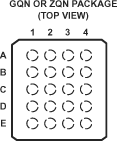
Table 1. Pin Assignments
| 1 | 2 | 3 | 4 | |
|---|---|---|---|---|
| A | A1 | DIR | VCC | OE |
| B | A3 | B2 | A2 | B1 |
| C | A5 | A4 | B4 | B3 |
| D | A7 | B6 | A6 | B5 |
| E | GND | A8 | B8 | B7 |