SCAS319J November 1993 – December 2014 SN74LVCH16652A
PRODUCTION DATA.
- 1 Features
- 2 Applications
- 3 Description
- 4 Simplified Schematic
- 5 Revision History
- 6 Pin Configuration and Functions
-
7 Specifications
- 7.1 Absolute Maximum Ratings
- 7.2 ESD Ratings
- 7.3 Recommended Operating Conditions
- 7.4 Thermal Information
- 7.5 Electrical Characteristics
- 7.6 Timing Requirements, 40°C to 85°C
- 7.7 Timing Requirements, 40°C to 125°C
- 7.8 Switching Characteristics, 40°C to 85°C
- 7.9 Switching Characteristics, 40°C to 125°C
- 7.10 Operating Characteristics
- 7.11 Typical Characteristics
- 8 Parameter Measurement Information
- 9 Detailed Description
- 10Application and Implementation
- 11Power Supply Recommendations
- 12Layout
- 13Device and Documentation Support
- 14Mechanical, Packaging, and Orderable Information
封装选项
请参考 PDF 数据表获取器件具体的封装图。
机械数据 (封装 | 引脚)
- DGG|56
- DL|56
- DGV|56
散热焊盘机械数据 (封装 | 引脚)
订购信息
6 Pin Configuration and Functions
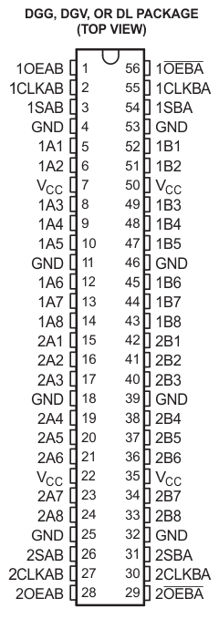
Pin Functions
| PIN | TYPE | DESCRIPTION | |
|---|---|---|---|
| NO. | NAME | ||
| 1 | 1OEAB | I | 1OEAB Input. Active-high enable for A-to-B directional data. |
| 2 | 1CLKAB | I | 1CLKAB Input. Clock input for D flip-flop from A to B. |
| 3 | 1SAB | I | 1SAB Input. Data select from A to B: A high level selects stored data and a low-level selects real-time data. |
| 4 | GND | — | GND |
| 5 | 1A1 | I/O | 1A1 Input/Output |
| 6 | 1A2 | I/O | 1A2 Input/Output |
| 7 | VCC | — | Power Pin |
| 8 | 1A3 | I/O | 1A3 Input/Output |
| 9 | 1A4 | I/O | 1A4 Input/Output |
| 10 | 1A5 | I/O | 1A5 Input/Output |
| 11 | GND | — | Ground Pin |
| 12 | 1A6 | I/O | 1A6 Input/Output |
| 13 | 1A7 | I/O | 1A7 Input/Output |
| 14 | 1A8 | I/O | 1A8 Input/Output |
| 15 | 2A1 | I/O | 2A1 Input/Output |
| 16 | 2A2 | I/O | 2A2 Input/Output |
| 17 | 2A3 | I/O | 2A3 Input/Output |
| 18 | GND | — | Ground Pin |
| 19 | 2A4 | I/O | 2A4 Input/Output |
| 20 | 2A5 | I/O | 2A5 Input/Output |
| 21 | 2A6 | I/O | 2A6 Input/Output |
| 22 | VCC | — | Power Pin |
| 23 | 2A7 | I/O | 2A7 Input/Output |
| 24 | 2A8 | I/O | 2A8 Input/Output |
| 25 | GND | — | Ground Pin |
| 26 | 2SAB | I | 2SAB Input. Data select from A to B: A high level selects stored data and a low-level selects real-time data. |
| 27 | 2CLKAB | I | 2CLKAB Input. Clock input for D flip-flop from A to B. |
| 28 | 2OEAB | I | 2OEAB Input. Active-high enable for A-to-B directional data. |
| 29 | 2OEBA | I | 2OEBA Input. Active-low enable for B-to-A directional data. |
| 30 | 2CLKBA | I | 2CLKBA Input. Clock input for D flip-flop from B to A. |
| 31 | 2SBA | I | 2SBA Input. Data select from B to A: A high level selects stored data and a low-level selects real-time data. |
| 32 | GND | — | Ground Pin |
| 33 | 2B8 | I/O | 2B8 Input/Output |
| 34 | 2B7 | I/O | 2B7 Input/Output |
| 35 | VCC | — | Power Pin |
| 36 | 2B6 | I/O | 2B6 Input/Output |
| 37 | 2B5 | I/O | 2B5 Input/Output |
| 38 | 2B4 | I/O | 2B4 Input/Output |
| 39 | GND | - | Ground Pin |
| 40 | 2B3 | I/O | 2B3 Input/Output |
| 41 | 2B2 | I/O | 2B2 Input/Output |
| 42 | 2B1 | — | 2B1 Input/Output |
| 43 | 1B8 | I/O | 1B8 Input/Output |
| 44 | 1B7 | I/O | 1B7 Input/Output |
| 45 | 1B6 | I/O | 1B6 Input/Output |
| 46 | GND | — | Ground Pin |
| 47 | 1B5 | I/O | 1B5 Input/Output |
| 48 | 1B4 | I/O | 1B4 Input/Output |
| 49 | 1B3 | I/O | 1B3 Input/Output |
| 50 | VCC | — | Power Pin |
| 51 | 1B2 | I/O | 1B2 Input/Output |
| 52 | 1B1 | I/O | 1B1 Input/Output |
| 53 | GND | — | Ground Pin |
| 54 | 1SBA | i | 1SBA Input. Data select from B to A: A high-level selects stored data and a low-level selects real-time data. |
| 55 | 1CLKBA | I | 1CLKBA Input. Clock input for D flip-flop from B to A. |
| 56 | 1OEBA | I | 1OEBA Input. Active-low enable for B-to-A directional data. |