SCAS757B December 2003 – September 2014 SN74LVCH16374A
PRODUCTION DATA.
- 1 Features
- 2 Applications
- 3 Simplified Schematic
- 4 Revision History
- 5 Pin Configuration and Functions
- 6 Specifications
- 7 Detailed Description
- 8 Application and Implementation
- 9 Power Supply Recommendations
- 10Layout
- 11Device and Documentation Support
- 12Mechanical, Packaging, and Orderable Information
封装选项
机械数据 (封装 | 引脚)
散热焊盘机械数据 (封装 | 引脚)
订购信息
7 Detailed Description
7.1 Overview
This 16-bit edge-triggered D-type flip-flop is designed for 1.65-V to 3.6-V VCC operation.
A buffered output-enable (OE) input can be used to place the eight outputs in either a normal logic state (high or low logic levels) or the high-impedance state. In the high-impedance state, the outputs neither load nor drive the bus lines significantly. The high-impedance state and increased drive provide the capability to drive bus lines without interface or pull-up components.
OE does not affect internal operations of the flip-flop. Old data can be retained or new data can be entered while the outputs are in the high-impedance state.
To ensure the high-impedance state during power up or power down, OE should be tied to VCC through a pull-up resistor; the minimum value of the resistor is determined by the current-sinking capability of the driver.
Inputs can be driven from either 3.3-V or 5-V devices. This feature allows the use of this device as a translator in a mixed 3.3-V/5-V system environment.
Active bus-hold circuitry holds unused or not driven inputs at a valid logic state. Use of pull-up or pull-down resistors with the bus-hold circuitry is not recommended.
The SN74LVCH16374A is particularly suitable for implementing buffer registers, I/O ports, bidirectional bus drivers, and working registers. It can be used as two 8-bit flip-flops or one 16-bit flip-flop. On the positive transition of the clock (CLK) input, the Q outputs of the flip-flop take on the logic levels set up at the data (D) inputs.
This device is fully specified for partial-power-down applications using Ioff. The Ioff circuitry disables the outputs, preventing damaging current backflow through the device when it is powered down.
7.2 Functional Block Diagram
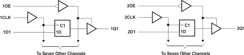 Figure 4. Logic Diagram (Positive Logic)
7.3 Feature Description
- Wide operating voltage range
- Operates from 1.65 V to 3.6 V
- Allows down voltage translation
- Inputs accept voltages to 5.5 V
- Ioff feature
- Allows voltages on the inputs and outputs when VCC is 0 V
- Bus Hold on data inputs eliminates the need for external pull-up or pull-down resistors
7.4 Device Functional Modes
Table 3. Function Table
(Each Flip-Flop)
| INPUTS | OUTPUT Q |
||
|---|---|---|---|
| OE | CLK | D | |
| L | ↑ | H | H |
| L | ↑ | L | L |
| L | H or L | X | Q0 |
| H | X | X | Z |