SCES495C October 2003 – June 2014 SN74LVCH16245A
PRODUCTION DATA.
- 1 Features
- 2 Applications
- 3 Description
- 4 Simplified Schematic
- 5 Revision History
- 6 Pin Configuration and Functions
- 7 Specifications
- 8 Parameter Measurement Information
- 9 Detailed Description
- 10Application and Implementation
- 11Power Supply Recommendations
- 12Layout
- 13Device and Documentation Support
- 14Mechanical, Packaging, and Orderable Information
封装选项
机械数据 (封装 | 引脚)
散热焊盘机械数据 (封装 | 引脚)
订购信息
9 Detailed Description
9.1 Overview
The SN74LVCH16245A device is designed for asynchronous communication between data buses. The logic levels of the direction-control (DIR) input and the output-enable (OE) input activate either the B-port outputs or the A-port outputs or place both output ports into the high-impedance mode. The device transmits data from the A bus to the B bus when the B-port outputs are activated, and from the B bus to the A bus when the A-port outputs are activated. The input circuitry on both A and B ports always is active and must have a logic high or low level applied to prevent excess ICC and ICCZ.
Active bus-hold circuitry holds unused or undriven data inputs at a valid logic state. Use of pullup or pulldown resistors with the bus-hold circuitry is not recommended. The bus-hold circuitry is part of the input circuit and is not disabled by OE or DIR.
To ensure the high-impedance state during power up or power down, OE should be tied to VCC through a pullup resistor; the minimum value of the resistor is determined by the current-sinking capability of the driver.
Inputs can be driven from either 3.3-V or 5-V devices. This feature allows the use of these devices as translators in a mixed 3.3-V and 5-V system environment.
This device is fully specified for partial-power-down applications using Ioff. The Ioff circuitry disables the outputs, thus preventing damaging current backflow through the device when it is powered down.
9.2 Functional Block Diagram
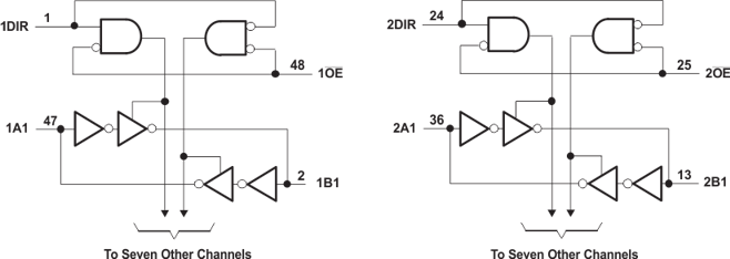 Figure 4. Logic Diagram (Positive Logic)
9.3 Feature Description
- Wide operating voltage range
- Operates from 1.65 V to 3.6 V
- Allows down voltage translation
- Inputs accept voltages to 5.5 V
- Ioff feature
- Allows voltages on the inputs and outputs when VCC is 0 V
9.4 Device Functional Modes
Table 3. Function Table(1)
(Each 8-bit Section)
| CONTROL INPUTS | OPERATION | |
|---|---|---|
| OE | DIR | |
| L | L | B data to A bus |
| L | H | A data to B bus |
| H | X | Isolation |