SCAS298N January 1993 – June 2014 SN54LVC541A , SN74LVC541A
PRODUCTION DATA.
- 1 Features
- 2 Applications
- 3 Description
- 4 Simplified Schematic
- 5 Revision History
- 6 Pin Configuration and Functions
-
7 Specifications
- 7.1 Absolute Maximum Ratings
- 7.2 Handling Ratings
- 7.3 Recommended Operating Conditions
- 7.4 Thermal Information
- 7.5 Electrical Characteristics—DC Limit Changes
- 7.6 Switching Characteristics—AC Limit Changes
- 7.7 Switching Characteristics, SN74LVC541A -40°C to 85°C
- 7.8 Switching Characteristics, SN74LVC541A -40°C to 125°C
- 7.9 Operating Characteristics
- 7.10 Typical Characteristics
- 8 Parameter Measurement Information
- 9 Detailed Description
- 10Application and Implementation
- 11Power Supply Recommendations
- 12Layout
- 13Device and Documentation Support
- 14Mechanical, Packaging, and Orderable Information
封装选项
请参考 PDF 数据表获取器件具体的封装图。
机械数据 (封装 | 引脚)
- DGV|20
- DB|20
- NS|20
- DW|20
- PW|20
- RGY|20
散热焊盘机械数据 (封装 | 引脚)
- RGY|20
订购信息
10 Application and Implementation
10.1 Application Information
The SN74LVC541A is a high-drive CMOS device that can be used for a multitude of bus-interface type applications where the data needs to be retained or latched. It can produce 24 mA of drive current at 3.3 V. Therefore, this device is ideal for driving multiple outputs and for high-speed applications up to 100 Mhz. The inputs are 5.5 V tolerant allowing the device to translate down to VCC.
10.2 Typical Application
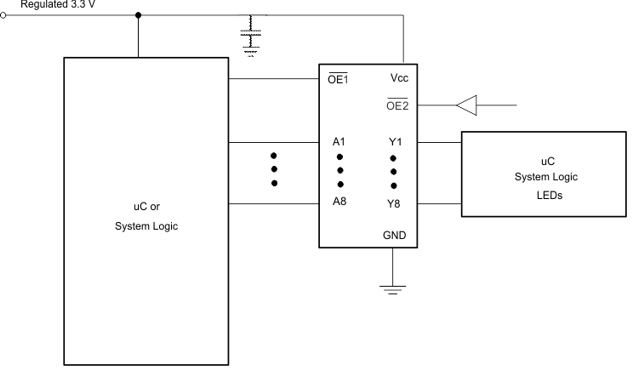 Figure 4. Typical Application Diagram
10.2.1 Design Requirements
This device uses CMOS technology and has balanced output drive. Care should be taken to avoid bus contention because it can drive currents that would exceed maximum limits. The high drive will also create fast edges into light loads; therefore, routing and load conditions should be considered to prevent ringing.
10.2.2 Detailed Design Procedure
- Recommended Input Conditions
- Rise time and fall time specs: See (Δt/ΔV) in the Recommended Operating Conditions table.
- Specified high and low levels: See (VIH and VIL) in the Recommended Operating Conditions table.
- Inputs are overvoltage tolerant allowing them to go as high as 5.5 V at any valid VCC.
- Recommend Output Conditions
- Load currents should not exceed 25 mA per output and 50 mA total for the part.
- Outputs should not be pulled above VCC.
10.2.3 Application Curves
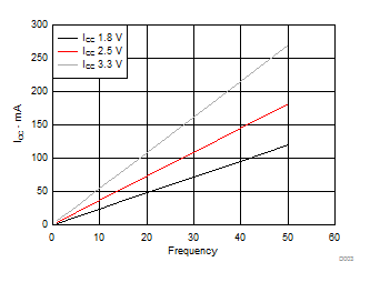 Figure 5. ICC vs Frequency