ZHCS198B June 2011 – October 2021 SN74LVC2G66-Q1
PRODUCTION DATA
- 1 特性
- 2 应用
- 3 说明
- 4 Revision History
- 5 Ordering Information
- 6 Pin Configuration and Functions
- 7 Specifications
- 8 Parameter Measurement Information
- 9 Detailed Description
- 10Application and Implementation
- 11Power Supply Recommendations
- 12Layout
- 13Device and Documentation Support
- 14Mechanical, Packaging, and Orderable Information
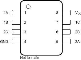
6 Pin Configuration and Functions
 Figure 6-1 DCU Package8-Pin VSSOPTop View
Pin Functions
| PIN | I/O | DESCRIPTION | |
|---|---|---|---|
| NAME | NAME | ||
| 1A | 1 | I/O | Bidirectional signal to be switched |
| 1B | 2 | I/O | Bidirectional signal to be switched |
| 2C | 3 | I | Controls the switch (L = OFF, H = ON) |
| GND | 4 | — | Ground pin |
| 2A | 5 | I/O | Bidirectional signal to be switched |
| 2B | 6 | I/O | Bidirectional signal to be switched |
| 1C | 7 | I | Controls the switch (L = OFF, H = ON) |
| VCC | 8 | — | Power Pin |