SCES381N January 2002 – January 2015 SN74LVC2G17 , SN74LVC2G17
PRODUCTION DATA.
- 1 Features
- 2 Applications
- 3 Simplified Schematic
- 4 Revision History
- 5 Pin Configuration and Functions
- 6 Specifications
- 7 Parameter Measurement Information
- 8 Detailed Description
- 9 Application and Implementation
- 10Power Supply Recommendations
- 11Layout
- 12Device and Documentation Support
- 13Mechanical, Packaging, and Orderable Information
封装选项
机械数据 (封装 | 引脚)
散热焊盘机械数据 (封装 | 引脚)
- DRY|6
订购信息
8 Detailed Description
8.1 Overview
NanoFree™ package technology is a major breakthrough in IC packaging concepts, using the die as the package.
This device is fully specified for partial-power-down applications using Ioff. The Ioff circuitry disables the outputs, preventing damaging current backflow through the device when it is powered down.
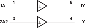
8.2 Functional Block Diagram
8.3 Feature Description
- 1.65 V to 5.5 V operating voltage range
- Allows down voltage translation
- 5 V to 3.3 V
- 5 V or 3.3 V to 1.8 V
- Inputs accept voltages to 5.5 V
- 5-V tolerance on input pin
- Ioff feature
- Allows voltage on the inputs and outputs when VCC is 0 V
- Able to reduce leakage when VCC is 0 V
- Schmitt-Trigger Input can improve the noise immunity capability
8.4 Device Functional Modes
| INPUT A |
OUTPUT Y |
|---|---|
| H | H |
| L | L |