SCAS572L April 1996 – July 2014 SN74LVC2244A
PRODUCTION DATA.
- 1 Features
- 2 Applications
- 3 Description
- 4 Simplified Schematic
- 5 Revision History
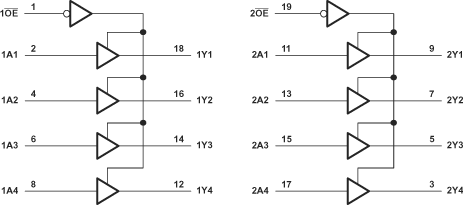
- 6 Pin Configuration and Functions
- 7 Specifications
- 8 Detailed Description
- 9 Application and Implementation
- 10Power Supply Recommendations
- 11Layout
- 12Device and Documentation Support
- 13Mechanical, Packaging, and Orderable Information
封装选项
请参考 PDF 数据表获取器件具体的封装图。
机械数据 (封装 | 引脚)
- DGV|20
- DB|20
- DBQ|20
- NS|20
- DW|20
- PW|20
散热焊盘机械数据 (封装 | 引脚)
订购信息
8 Detailed Description
8.1 Overview
This octal buffer and line driver is designed for 1.65-V to 3.6-V VCC operation. The SN74LVC2244A device is organized as two 4-bit line drivers with separate output-enable (OE) inputs. When OE is low, the device passes data from the A inputs to the Y outputs. When OE is high, the outputs are in the high-impedance state. The outputs, which are designed to sink up to 12 mA, include equivalent 26-ohm resistors to reduce overshoot and undershoot.
8.2 Functional Block Diagram
8.3 Feature Description
- Wide operating voltage range
- Operates from 1.65 V to 3.6 V
- Allows down voltage translation
- Inputs accept voltages to 5.5 V
- Ioff Feature
- Allows voltages on the inputs and outputs when VCC is 0 V
8.4 Device Functional Modes
Table 1. Function Table
(Each Buffer)
| INPUTS | OUTPUT Y |
|
|---|---|---|
| OE | A | |
| L | H | H |
| L | L | L |
| H | X | Z |