ZHCSHF2E August 2004 – January 2018 SN74LVC1G139
PRODUCTION DATA.
- 1 特性
- 2 应用
- 3 说明
- 4 修订历史记录
- 5 Pin Configuration and Functions
- 6 Specification
- 7 Typical Characteristics
- 8 Parameter Measurement Information
- 9 Detailed Description
- 10Application and Implementation
- 11Power Supply Recommendations
- 12Layout
- 13器件和文档支持
- 14机械、封装和可订购信息
封装选项
机械数据 (封装 | 引脚)
散热焊盘机械数据 (封装 | 引脚)
订购信息
5 Pin Configuration and Functions
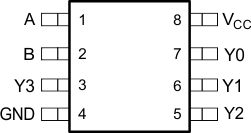
DCT Package
8-Pin SM8
Top View

DCU Package
8-Pin VSSOP
Top View

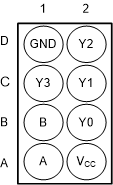
Pin Functions
| PIN | I/O | DESCRIPTION | ||
|---|---|---|---|---|
| NAME | DCT, DCU | YZP | ||
| A | 1 | A1 | I | Adress input, bit 0 |
| B | 2 | B1 | I | Adress input, bit 1 |
| Y3 | 3 | C1 | O | Output 3, low when B is high and A is high |
| GND | 4 | D1 | — | Ground |
| Y2 | 5 | D2 | O | Output 2, low when B is high and A is low |
| Y1 | 6 | C2 | O | Output 1, low when B is low and A is high |
| Y0 | 7 | B2 | O | Output 0, low when B is low and A is low |
| VCC | 8 | A2 | — | Power pin |
