SCAS758B DECember 2003 – June 2014 SN74LVC162244A
PRODUCTION DATA.
- 1 Features
- 2 Applications
- 3 Description
- 4 Simplified Schematic
- 5 Revision History
- 6 Pin Configuration and Functions
- 7 Specifications
- 8 Parameter Measurement Information
- 9 Detailed Description
- 10Application and Implementation
- 11Power Supply Recommendations
- 12Layout
- 13Device and Documentation Support
- 14Mechanical, Packaging, and Orderable Information
封装选项
机械数据 (封装 | 引脚)
散热焊盘机械数据 (封装 | 引脚)
订购信息
6 Pin Configuration and Functions
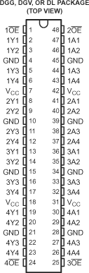
Pin Functions
| PIN | I/O | DESCRIPTION | |
|---|---|---|---|
| NAME | NO. | ||
| 1OE | 1 | I | Output Enable 1 (input) |
| 1Y1 | 2 | O | 1Y1 Output |
| 1Y2 | 3 | O | 1Y2 Output |
| GND | 4 | – | Ground pin |
| 1Y3 | 5 | O | 1Y3 Output |
| 1Y4 | 6 | O | 1Y4 Output |
| VCC | 7 | – | Power pin |
| 2Y1 | 8 | O | 2Y1 Output |
| 2Y2 | 9 | O | 2Y2 Output |
| GND | 10 | – | Ground pin |
| 2Y3 | 11 | O | 2Y3 Output |
| 2Y4 | 12 | O | 2Y4 Output |
| 3Y1 | 13 | O | 3Y1 Output |
| 3Y2 | 14 | O | 3Y2 Output |
| GND | 15 | – | Ground pin |
| 3Y3 | 16 | O | 3Y3 Output |
| 3Y4 | 17 | O | 3Y4 Output |
| VCC | 18 | – | Power pin |
| 4Y1 | 19 | O | 4Y1 Output |
| 4Y2 | 20 | O | 4Y2 Output |
| GND | 21 | – | Ground pin |
| 4Y3 | 22 | O | 4Y3 Output |
| 4Y4 | 23 | O | 4Y4 Output |
| 4OE | 24 | I | Output Enable 4 (input) |
| 3OE | 25 | I | Output Enable 3 (input) |
| 4A4 | 26 | I | 4A4 Input |
| 4A3 | 27 | I | 4A3 Input |
| GND | 28 | – | Ground pin |
| 4A2 | 29 | I | 4A2 Input |
| 4A1 | 30 | I | 4A1 Input |
| VCC | 31 | – | Power pin |
| 3A4 | 32 | I | 3A4 Input |
| 3A3 | 33 | I | 3A3 Input |
| GND | 34 | – | Ground pin |
| 3A2 | 35 | I | 3A2 Input |
| 3A1 | 36 | I | 3A1 Input |
| 2A4 | 37 | I | 2A4 Input |
| 2A3 | 38 | I | 2A3 Input |
| GND | 39 | – | Ground pin |
| 2A2 | 40 | I | 2A2 Input |
| 2A1 | 41 | I | 2A1 Input |
| VCC | 42 | – | Power pin |
| 1A4 | 43 | I | 1A4 Input |
| 1A3 | 44 | I | 1A3 Input |
| GND | 45 | – | Ground pin |
| 1A2 | 46 | I | 1A2 Input |
| 1A1 | 47 | I | 1A1 Input |
| 2OE | 48 | I | Output Enable 2 (Input) |
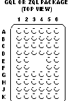
Table 1. 3Pin Assignments(1)
(56-Ball GQL or ZQL Package)
| 1 | 2 | 3 | 4 | 5 | 6 | |
|---|---|---|---|---|---|---|
| A | 1OE | NC | NC | NC | NC | 2OE |
| B | 1Y2 | 1Y1 | GND | GND | 1A1 | 1A2 |
| C | 1Y4 | 1Y3 | VCC | VCC | 1A3 | 1A4 |
| D | 2Y2 | 2Y1 | GND | GND | 2A1 | 2A2 |
| E | 2Y4 | 2Y3 | 2A3 | 2A4 | ||
| F | 3Y1 | 3Y2 | 3A2 | 3A1 | ||
| G | 3Y3 | 3Y4 | GND | GND | 3A4 | 3A3 |
| H | 4Y1 | 4Y2 | VCC | VCC | 4A2 | 4A1 |
| J | 4Y3 | 4Y4 | GND | GND | 4A4 | 4A3 |
| K | 4OE | NC | NC | NC | NC | 3OE |
(1) NC - No internal connection
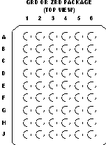
Table 2. Pin Assignments(1)
(54-Ball GRD or ZRD Package)
| 1 | 2 | 3 | 4 | 5 | 6 | |
|---|---|---|---|---|---|---|
| A | 1Y1 | NC | 1OE | 2OE | NC | 1A1 |
| B | 1Y3 | 1Y2 | NC | NC | 1A2 | 1A3 |
| C | 2Y1 | 1Y4 | VCC | VCC | 1A4 | 2A1 |
| D | 2Y3 | 2Y2 | GND | GND | 2A2 | 2A3 |
| E | 3Y1 | 2Y4 | GND | GND | 2A4 | 3A1 |
| F | 3Y3 | 3Y2 | GND | GND | 3A2 | 3A3 |
| G | 4Y1 | 3Y4 | VCC | VCC | 3A4 | 4A1 |
| H | 4Y3 | 4Y2 | NC | NC | 4A2 | 4A3 |
| J | 4Y4 | NC | 4OE | 3OE | NC | 4A4 |
(1) NC - No internal connection