SCLS520E August 2003 – January 2015 SN74LV4051A-Q1
PRODUCTION DATA.
- 1 Features
- 2 Applications
- 3 Description
- 4 Revision History
- 5 Pin Configuration and Functions
- 6 Specifications
- 7 Parameter Measurement Information
- 8 Detailed Description
- 9 Application and Implementation
- 10Power Supply Recommendations
- 11Layout
- 12Device and Documentation Support
- 13Mechanical, Packaging, and Orderable Information
封装选项
请参考 PDF 数据表获取器件具体的封装图。
机械数据 (封装 | 引脚)
- PW|16
- DW|16
- D|16
散热焊盘机械数据 (封装 | 引脚)
订购信息
9 Application and Implementation
NOTE
Information in the following applications sections is not part of the TI component specification, and TI does not warrant its accuracy or completeness. TI’s customers are responsible for determining suitability of components for their purposes. Customers should validate and test their design implementation to confirm system functionality.
9.1 Application Information
A multiplexer is used in applications where multiple signals share a resource. In the example below, several different sensors are connected to the analog-to-digital converter (ADC) of a microcontroller unit (MCU).
9.2 Typical Application
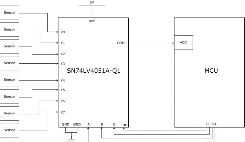 Figure 11. Example of Multiplexer Use With Analog Sensors and the ADC of an MCU
9.2.1 Design Requirements
Designing with the SN74LV4051A-Q1 device requires a stable input voltage between 2 V (see Recommended Operating Conditions for details) and 5.5 V. Another important design consideration is the characteristics of the signal being multiplexed, to ensure no important information is lost due to timing or incompatibility with this device.
9.2.2 Detailed Design Procedure
Normally, processing eight different analog signals would require eight separate ADCs, but Figure 11 shows how to achieve this using only one ADC and four GPIOs (general-purpose input/outputs).