ZHCSPI2A July 2020 – December 2021 SN74HCS259-Q1
PRODUCTION DATA
- 1 特性
- 2 应用
- 3 说明
- 4 Revision History
- 5 Pin Configuration and Functions
- 6 Specifications
- 7 Parameter Measurement Information
- 8 Detailed Description
- 9 Application and Implementation
- 10Power Supply Recommendations
- 11Layout
- 12Device and Documentation Support
- 13Mechanical, Packaging, and Orderable Information
封装选项
机械数据 (封装 | 引脚)
散热焊盘机械数据 (封装 | 引脚)
- BQB|16
订购信息
5 Pin Configuration and Functions
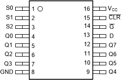
 D or PW Package
16-Pin SOIC or TSSOP
Top View
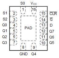
 WBQB Package
16-Pin WQFN
Top View
Pin Functions
| PIN | I/O(2) | DESCRIPTION | |
|---|---|---|---|
| SOIC or TSSOP NO. | NAME | ||
| 1 | S0 | I | Address select 0 |
| 2 | S1 | I | Address select 1 |
| 3 | S2 | I | Address select 2 |
| 4 | Q0 | O | Output 0 |
| 5 | Q1 | O | Output 1 |
| 6 | Q2 | O | Output 2 |
| 7 | Q3 | O | Output 3 |
| 8 | GND | — | Ground |
| 9 | Q4 | O | Output 4 |
| 10 | Q5 | O | Output 5 |
| 11 | Q6 | O | Output 6 |
| 12 | Q7 | O | Output 7 |
| 13 | D | I | Data input |
| 14 | G | I | Enable, active low |
| 15 | CLR | O | Clear input, active low |
| 16 | VCC | — | Positive supply |
| Thermal Pad (1) | — | The thermal pad can be connected to GND or left floating. Do not connect to any other signal or supply. | |
(1) WBQB package only.
(2) Signal Types: I = Input, O =
Output, I/O = Input or Output.