SCDS003P November 1992 – December 2015 SN74CBT3383
- 1 Features
- 2 Applications
- 3 Description
- 4 Revision History
- 5 Pin Configuration and Functions
- 6 Specifications
- 7 Parameter Measurement Information
- 8 Detailed Description
- 9 Application and Implementation
- 10Power Supply Recommendations
- 11Layout
- 12Device and Documentation Support
- 13Mechanical, Packaging, and Orderable Information
封装选项
请参考 PDF 数据表获取器件具体的封装图。
机械数据 (封装 | 引脚)
- DBQ|24
- DW|24
- DB|24
- PW|24
散热焊盘机械数据 (封装 | 引脚)
订购信息
9 Application and Implementation
NOTE
Information in the following applications sections is not part of the TI component specification, and TI does not warrant its accuracy or completeness. TI’s customers are responsible for determining suitability of components for their purposes. Customers should validate and test their design implementation to confirm system functionality.
9.1 Application Information
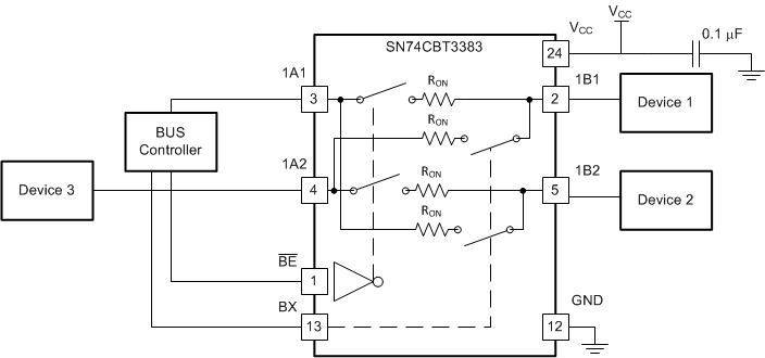
The SN74CBT3383 can be used to multiplex up to 5 channels simultaneously in a 2:1 configuration. The application shown here is a 2-bit bus being multiplexed between two devices. The BE and BX pins are used to control the chip from the bus controller. This is a very generic example, and could apply to many situations. If an application requires only one bit control or exchange, remember to tie the unused bit to high or low. By using another bus controller you can enable exchange across A1 and A2 to B1 and B2, allowing for greater system communication.
9.2 Typical Application
 Figure 3. 1:2 Multiplexer or Bus and Selector Using 1 Bus Controller
9.2.1 Design Requirements
- Recommended Input Conditions:
- For specified high and low levels, see VIH and VIL in Recommended Operating Conditions.
- Recommended Output Conditions:
- Load currents must not exceed 128 mA per channel.
- Frequency Selection Criterion:
- Maximum frequency tested is 200 MHz.
- Added trace resistance and capacitance can reduce maximum frequency capability; use layout practices as directed in Layout.
9.2.2 Detailed Design Procedure
The 2-bit bus is connected directly to the 1A1, 1A2 on the SN74CBT3383, which essentially combines in the bus controller to form a single input or split bus bits. When BE is low and BX is low, the selected bus is using 1A1 and 1B1 as inputs and outputs. This means that Device 1 is connected to the bus controller and Device 2 is connected to Device 3 when BE is low and BX is low. While keeping BE low and using BX high, we can enable communication from the bus controller to Device 2 and from Device 1 to Device 3. This setup is especially useful when two controllers or devices need to share the same data from Device 1 and Device 2 and the bus addresses are limited or hard coded.
The 0.1-μF capacitor on VCC is a decoupling capacitor and should be placed as close as possible to the device.
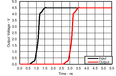
9.2.3 Application Curve

| VCC = 4.5 V |