SCES644D MARCH 2006 – December 2015 SN74AUP1G74
PRODUCTION DATA.
- 1 Features
- 2 Applications
- 3 Description
- 4 Revision History
- 5 Pin Configuration and Functions
-
6 Specifications
- 6.1 Absolute Maximum Ratings
- 6.2 ESD Ratings
- 6.3 Recommended Operating Conditions
- 6.4 Thermal Information
- 6.5 Electrical Characteristics, TA = 25°C
- 6.6 Electrical Characteristics, TA = -40°C to +85°C
- 6.7 Timing Requirements
- 6.8 Switching Characteristics, CL = 5 pF
- 6.9 Switching Characteristics, CL = 10 pF
- 6.10 Switching Characteristics, CL = 15 pF
- 6.11 Switching Characteristics, CL = 30 pF
- 6.12 Operating Characteristics
- 6.13 Typical Characteristics
- 7 Parameter Measurement Information
- 8 Detailed Description
- 9 Application and Implementation
- 10Power Supply Recommendations
- 11Layout
- 12Device and Documentation Support
- 13Mechanical, Packaging, and Orderable Information
封装选项
机械数据 (封装 | 引脚)
散热焊盘机械数据 (封装 | 引脚)
订购信息
8 Detailed Description
8.1 Overview
This single positive-edge-triggered D-type flip-flop is designed for 0.8-V to 3.6-V VCC operation.
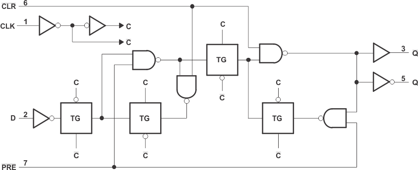
A low level at the preset (PRE) or clear (CLR) input sets or resets the outputs, regardless of the levels of the other inputs. When PRE and CLR are inactive (high), data at the data (D) input meeting the setup time requirements is transferred to the outputs on the positive-going edge of the clock pulse. Clock triggering occurs at a voltage level and is not related directly to the rise time of the clock pulse. Following the hold-time interval, data at the D input can be changed without affecting the levels at the outputs. When both the CLR and PRE inputs are set low, the CLR input will override the PRE input.
NanoStar package technology is a major breakthrough in IC packaging concepts, using the die as the package.
This device is fully specified for partial-power-down applications using Ioff. The Ioff circuitry disables the outputs, preventing damaging current backflow through the device when it is powered down.
8.2 Functional Block Diagram

8.3 Feature Description
This device is available in the Texas Instrument's NanoStar package. It has low static-power consumption of
0.9 uA maximum. It has low noise with overshoot and undershoot at less than ten percent of VCC. It supports partial-power-down mode operation, which is specified by Ioff. The Schmitt-trigger inputs allow for slow or noisy input signals. The device has a wide operating voltage range of 0.8 V to 3.6 V, and is optimized for 3.3 V. It has low propagation delay of 5 ns maximum at 3.3 V.
8.4 Device Functional Modes
Table 1 lists the functional modes of the SN74AUP1G74.
Table 1. Function Table
| INPUTS | OUTPUTS | ||||
|---|---|---|---|---|---|
| PRE | CLR | CLK | D | Q | Q |
| L | H | X | X | H | L |
| X | L | X | X | L | H |
| H | H | ↑ | H | H | L |
| H | H | ↑ | L | L | H |
| H | H | L | X | Q0 | Q 0 |