SCES591J JULY 2004 – June 2014 SN74AUP1G07
PRODUCTION DATA.
- 1 Features
- 2 Applications
- 3 Description
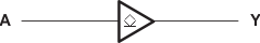
- 4 Simplified Schematic
- 5 Revision History
- 6 Pin Configuration and Functions
-
7 Specifications
- 7.1 Absolute Maximum Ratings
- 7.2 Handling Ratings
- 7.3 Recommended Operating Conditions
- 7.4 Thermal Information
- 7.5 Electrical Characteristics
- 7.6 Switching Characteristics, CL = 5 pF
- 7.7 Switching Characteristics, CL = 10 pF
- 7.8 Switching Characteristics, CL = 15 pF
- 7.9 Switching Characteristics, CL = 30 pF
- 7.10 Operating Characteristics
- 7.11 Typical Characteristics
- 8 Parameter Measurement Information
- 9 Detailed Description
- 10Application and Implementation
- 11Power Supply Recommendations
- 12Layout
- 13Device and Documentation Support
- 14Mechanical, Packaging, and Orderable Information
9 Detailed Description
9.1 Overview
The SN74AUP1G07 device is a single buffer gate with open drain output that operates from 0.8 V to 3.6 V. The output of this single buffer/driver is open drain, and can be connected to other open-drain outputs to implement active-low wired-OR or active-high wired-AND functions.
The AUP family of devices has quiescent power consumption less than 1ua and comes in the ultra small DPW package. The DPW package technology is a major breakthrough in IC packaging. Its tiny 0.64 mm square footprint saves significant board space over other package options while still retaining the traditional manufacturing friendly lead pitch of 0.5 mm.
This device is fully specified for partial-power-down applications using Ioff. The Ioff circuitry disables the outputs, preventing damaging current backflow through the device when it is powered down. The Ioff feature also allows for live insertion.
9.2 Functional Block Diagram
9.3 Feature Description
- Wide operating VCC range of 0.8 V to 3.6 V
- 3.6-V I/O tolerant to support down translation
- Input hysteresis allows slow input transition and better switching noise immunity at the input
- Ioff feature allows voltages on the inputs and outputs when VCC is 0 V
- Low noise due to slower edge rates
9.4 Device Functional Modes
Table 1. Function Table
| INPUT A |
OUTPUT Y |
|---|---|
| H | H/Z |
| L | L |