SCES015M JULY 1995 – June 2015 SN74ALVCH16245
PRODUCTION DATA.
- 1 Features
- 2 Applications
- 3 Description
- 4 Revision History
- 5 Pin Configuration and Functions
- 6 Specifications
- 7 Parameter Measurement Information
- 8 Detailed Description
- 9 Application and Implementation
- 10Power Supply Recommendations
- 11Layout
- 12Device and Documentation Support
- 13Mechanical, Packaging, and Orderable Information
封装选项
请参考 PDF 数据表获取器件具体的封装图。
机械数据 (封装 | 引脚)
- DGG|48
- DL|48
- DGV|48
散热焊盘机械数据 (封装 | 引脚)
订购信息
1 Features
- Member of the Texas Instruments Widebus™ Family
- Operates From 1.65 V to 3.6 V
- Max tpd of 3 ns at 3.3 V
- ±24-mA Output Drive at 3.3 V
- Bus Hold on Data Inputs Eliminates the Need for External Pullup or Pulldown Resistors
- Latch-Up Performance Exceeds 250 mA Per
JESD 17 - ESD Protection Exceeds JESD 22
- 2000-V Human-Body Model (A114-A)
- 200-V Machine Model (A115-A)
2 Applications
- Cable Modem Termination Systems
- Servers
- LED Displays
- Network Switches
- Telecom Infrastructure
- Motor Drivers
- I/O Expanders
3 Description
This 16-bit (dual-octal) noninverting bus transceiver is designed for 1.65-V to 3.6-V VCC operation.
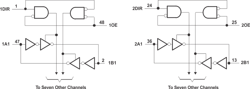
The SN74ALVCH16245 device is designed for asynchronous communication between two data buses. The logic levels of the direction-control (DIR) input and the output-enable (OE) input activate either the B-port outputs or the A-port outputs or place both output ports into the high-impedance mode. The device transmits data from the A bus to the B bus when the B-port outputs are activated, and from the B bus to the A bus when the A-port outputs are activated. The input circuitry on both A and B ports is always active and must have a logic high or low level applied to prevent excess ICC and ICCZ.
To ensure the high-impedance state during power up or power down, OE should be tied to VCC through a pullup resistor; the minimum value of the resistor is determined by the current-sinking capability of the driver.
Active bus-hold circuitry holds unused or undriven inputs at a valid logic state. Use of pullup or pulldown resistors with the bus-hold circuitry is not recommended.
Device Information(1)
| PART NUMBER | PACKAGE | BODY SIZE (NOM) |
|---|---|---|
| SN74ALVCH16245ZRD | BGA MICROSTAR JUNIOR (56) | 4.50 mm × 7.00 mm |
| SN74ALVCH16245ZQL | BGA MICROSTAR JUNIOR (54) | 5.50 mm × 8.00 mm |
| SN74ALVCH16245DGG | TSSOP (48) | 6.10 mm × 12.50 mm |
| SN74ALVCH16245DGV | TVSOP (48) | 4.40 mm × 9.70 mm |
| SN74ALVCH16245DL | SSOP (48) | 7.50 mm × 15.80 mm |
- For all available packages, see the orderable addendum at the end of the data sheet.
Logic Diagram (Positive Logic)
