SCLS336I January 2000 – August 2014 SN74AHCT16373
UNLESS OTHERWISE NOTED, this document contains PRODUCTION DATA.
- 1 Features
- 2 Applications
- 3 Description
- 4 Simplified Schematic
- 5 Revision History
- 6 Pin Configuration and Functions
- 7 Specifications
- 8 Parameter Measurement Information
- 9 Detailed Description
- 10Application and Implementation
- 11Power Supply Recommendations
- 12Layout
- 13Device and Documentation Support
- 14Mechanical, Packaging, and Orderable Information
封装选项
请参考 PDF 数据表获取器件具体的封装图。
机械数据 (封装 | 引脚)
- DGG|48
- DL|48
- DGV|48
散热焊盘机械数据 (封装 | 引脚)
订购信息
9 Detailed Description
9.1 Overview
The SNxAHCT16373 devices are 16-bit transparent D-type latches with 3-state outputs designed specifically for driving highly capacitive or relatively low-impedance loads. They are particularly suitable for implementing buffer registers, IO ports, bidirectional bus drivers, and working registers.
These devices can be used as two 8-bit latches or one 16-bit latch. When the latch-enable (LE) input is high, the Q outputs follow the data (D) inputs. When LE is taken low, the Q outputs are latched at the levels set up at the D inputs.
A buffered output-enable (OE) input can be used to place the eight outputs in either a normal logic state (high or low logic levels) or the high-impedance state. In the high-impedance state, the outputs neither load nor drive the bus lines significantly. The high-impedance state and the increased drive provide the capability to drive bus lines without need for interface or pullup components.
OE does not affect internal operations of the latch. Old data can be retained or new data can be entered while the outputs are in the high-impedance state.
To ensure the high-impedance state during power up or power down, OE should be tied to VCC through a pullup resistor; the minimum value of the resistor is determined by the current-sinking capability of the driver.
9.2 Functional Block Diagrams
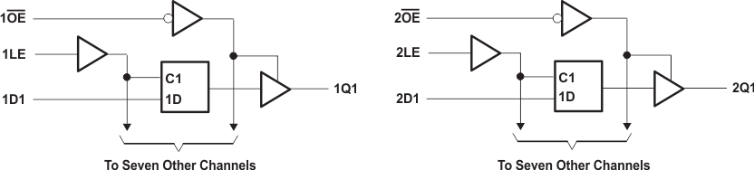 Figure 3. Logic Diagram (Positive Logic)
 Figure 4. Logic Symbol
9.3 Feature Description
- TTL inputs
- Lowered switching threshold allows up translation from 3.3 V to 5 V
- Slow edges reduce output ringing
9.4 Device Functional Modes
Table 1. Function Table
(Each 8-bit Latch)
| INPUTS | OUTPUT Q |
||
|---|---|---|---|
| OE | LE | D | |
| L | H | H | H |
| L | H | L | L |
| L | L | X | Q0 |
| H | X | X | Z |