SCLS336I January 2000 – August 2014 SN74AHCT16373
UNLESS OTHERWISE NOTED, this document contains PRODUCTION DATA.
- 1 Features
- 2 Applications
- 3 Description
- 4 Simplified Schematic
- 5 Revision History
- 6 Pin Configuration and Functions
- 7 Specifications
- 8 Parameter Measurement Information
- 9 Detailed Description
- 10Application and Implementation
- 11Power Supply Recommendations
- 12Layout
- 13Device and Documentation Support
- 14Mechanical, Packaging, and Orderable Information
封装选项
请参考 PDF 数据表获取器件具体的封装图。
机械数据 (封装 | 引脚)
- DGG|48
- DL|48
- DGV|48
散热焊盘机械数据 (封装 | 引脚)
订购信息
10 Application and Implementation
10.1 Application Information
The SN74AHCT16373 is a low-drive CMOS device that can be used for a multitude of bus interface type applications where output ringing is a concern. The low drive and slow edge rates will minimize overshoot and undershoot on the outputs. The input switching levels have been lowered to accommodate TTL inputs of 0.8-V VIL and 2-V VIH. This feature makes it ideal for translating up from 3.3 V to 5 V. Figure 6 shows this type of translation.
10.2 Typical Application
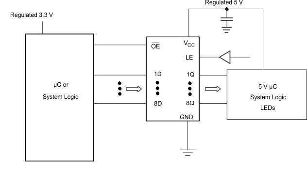 Figure 5. Typical Application Schematic
10.2.1 Design Requirements
This device uses CMOS technology and has balanced output drive. Care should be taken to avoid bus contention because it can drive currents that would exceed maximum limits. The high drive will also create fast edges into light loads so routing and load conditions should be considered to prevent ringing.
10.2.2 Detailed Design Procedure
- Recommended input conditions
- Rise time and fall time specs: See (Δt/ΔV) in the Recommended Operating Conditions table.
- Specified High and low levels: See (VIH and VIL) in the Recommended Operating Conditions table.
- Inputs are overvoltage tolerant allowing them to go as high as 5.5 V at any valid VCC
- Recommend output conditions
- Load currents should not exceed 25 mA per output and 75 mA total for the part
- Outputs should not be pulled above VCC
10.2.3 Application Curves
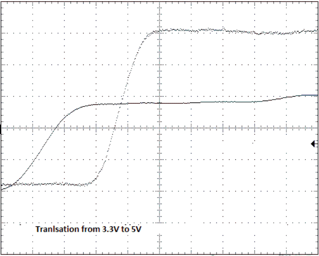 Figure 6. Up Translation