SCLS335K March 1996 – October 2014 SN74AHCT16245
PRODUCTION DATA.
- 1 Features
- 2 Applications
- 3 Description
- 4 Simplified Schematic
- 5 Revision History
- 6 Pin Configuration and Functions
- 7 Specifications
- 8 Parameter Measurement Information
- 9 Detailed Description
- 10Application and Implementation
- 11Power Supply Recommendations
- 12Layout
- 13Device and Documentation Support
- 14Mechanical, Packaging, and Orderable Information
封装选项
请参考 PDF 数据表获取器件具体的封装图。
机械数据 (封装 | 引脚)
- DGG|48
- DL|48
- DGV|48
散热焊盘机械数据 (封装 | 引脚)
订购信息
9 Detailed Description
9.1 Overview
The SN74AHCT16245 device is a 16-bit (dual-octal) noninverting 3-state transceiver designed for synchronous two-way communication between data buses. The control-function implementation minimizes external timing requirements.
This device can be used as two 8-bit transceivers or one 16-bit transceiver. It allows data transmission from the A bus to the B bus or from the B bus to the A bus, depending on the logic level at the direction-control (DIR) input. The output-enable (OE) input can be used to disable the device so that the buses are effectively isolated.
To ensure the high-impedance state during power up or power down, OE should be tied to VCC through a pullup resistor; the minimum value of the resistor is determined by the current-sinking capability of the driver.
9.2 Functional Block Diagrams
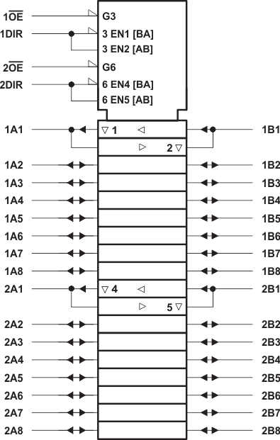
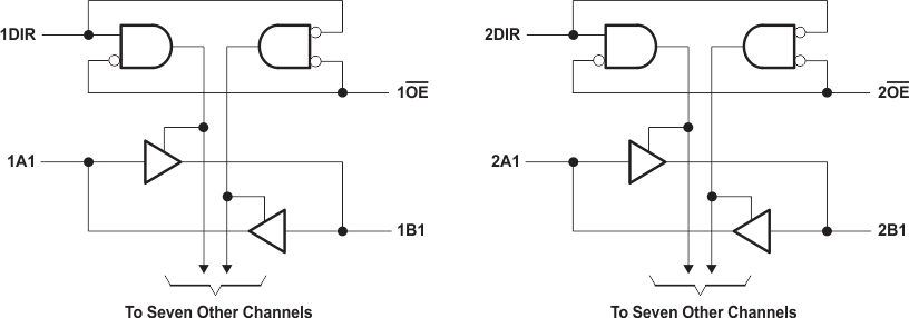 Figure 4. Logic Diagram (Positive Logic)
9.3 Feature Description
- TTL inputs
- Lowered switching threshold allows up translation 3.3 V to 5 V
- Slow edges reduce output ringing
9.4 Device Functional Modes
Table 1. Function Table
(Each 8-bit Transceiver)
| INPUTS | OPERATION | |
|---|---|---|
| OE | DIR | |
| L | L | B data to A bus |
| L | H | A data to B bus |
| H | X | Isolation |