SCLS242L October 1995 – September 2014 SN54AHC573 , SN74AHC573
PRODUCTION DATA.
- 1 Features
- 2 Applications
- 3 Description
- 4 Simplified Schematic
- 5 Revision History
- 6 Pin Configuration and Functions
-
7 Specifications
- 7.1 Absolute Maximum Ratings
- 7.2 Handling Ratings
- 7.3 Recommended Operating Conditions
- 7.4 Thermal Information
- 7.5 Electrical Characteristics
- 7.6 Timing Requirements, VCC = 3.3 V ± 0.3 V
- 7.7 Timing Requirements, VCC = 5 V ± 0.5 V
- 7.8 Switching Characteristics, VCC = 3.3 V ± 0.3 V
- 7.9 Switching Characteristics, VCC = 5 V ± 0.5 V
- 7.10 Noise Characteristics
- 7.11 Operating Characteristics
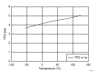
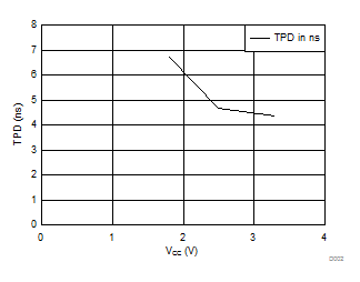
- 7.12 Typical Characteristics
- 8 Parameter Measurement Information
- 9 Detailed Description
- 10Application and Implementation
- 11Power Supply Recommendations
- 12Layout
- 13Device and Documentation Support
- 14Mechanical, Packaging, and Orderable Information
封装选项
请参考 PDF 数据表获取器件具体的封装图。
机械数据 (封装 | 引脚)
- DGV|20
- DB|20
- NS|20
- N|20
- DW|20
- PW|20
散热焊盘机械数据 (封装 | 引脚)
- PW|20
订购信息
7 Specifications
7.1 Absolute Maximum Ratings(1)
over operating free-air temperature range (unless otherwise noted)| MIN | MAX | UNIT | |||
|---|---|---|---|---|---|
| VCC | Supply voltage range | –0.5 | 7 | V | |
| VI | Input voltage range(2) | –0.5 | 7 | V | |
| VO | Output voltage range(2) | –0.5 | VCC + 0.5 | V | |
| IIK | Input clamp current | VI < 0 | –20 | mA | |
| IOK | Output clamp current | VO < 0 or VO > VCC | ±20 | mA | |
| IO | Continuous output current | VO = 0 to VCC | ±25 | mA | |
| Continuous current through VCC or GND | ±75 | mA | |||
(1) Stresses beyond those listed under Absolute Maximum Ratings may cause permanent damage to the device. These are stress ratings only, and functional operation of the device at these or any other conditions beyond those indicated under Recommended Operating Conditions is not implied. Exposure to absolute-maximum-rated conditions for extended periods may affect device reliability.
(2) The input and output voltage ratings may be exceeded if the input and output current ratings are observed.
7.2 Handling Ratings
| MIN | MAX | UNIT | |||
|---|---|---|---|---|---|
| Tstg | Storage temperature range | –65 | 150 | °C | |
| V(ESD) | Electrostatic discharge | Human body model (HBM), per ANSI/ESDA/JEDEC JS-001, all pins(1) | 0 | 2000 | V |
| Charged device model (CDM), per JEDEC specification JESD22-C101, all pins(2) | 0 | 1000 | |||
(1) JEDEC document JEP155 states that 500-V HBM allows safe manufacturing with a standard ESD control process.
(2) JEDEC document JEP157 states that 250-V CDM allows safe manufacturing with a standard ESD control process.
7.3 Recommended Operating Conditions
over operating free-air temperature range (unless otherwise noted)(1)(1) All unused inputs of the device must be held at VCC or GND to ensure proper device operation. Refer to the TI application report, Implications of Slow or Floating CMOS Inputs (SCBA004).
7.4 Thermal Information
| THERMAL METRIC(1) | SN74AHC573 | UNIT | ||||||
|---|---|---|---|---|---|---|---|---|
| DW | DB | DGV | N | NS | PW | |||
| 20 PINS | ||||||||
| RθJA | Junction-to-ambient thermal resistance | 79.4 | 97.9 | 117.2 | 53.3 | 79.2 | 103.3 | °C/W |
| RθJC(top) | Junction-to-case (top) thermal resistance | 45.7 | 59.6 | 32.7 | 40.0 | 45.7 | 37.8 | |
| RθJB | Junction-to-board thermal resistance | 46.9 | 53.1 | 58.7 | 34.2 | 46.8 | 54.3 | |
| ψJT | Junction-to-top characterization parameter | 18.7 | 21.3 | 1.15 | 26.4 | 19.3 | 2.9 | |
| ψJB | Junction-to-board characterization parameter | 46.5 | 52.7 | 58.0 | 34.1 | 46.4 | 53.8 | |
| RθJC(bot) | Junction-to-case (bottom) thermal resistance | n/a | n/a | n/a | n/a | n/a | n/a | |
(1) For more information about traditional and new thermal metrics, see the IC Package Thermal Metrics application report (SPRA953).
7.5 Electrical Characteristics
over recommended operating free-air temperature range (unless otherwise noted)| PARAMETER | TEST CONDITIONS | VCC | TA = 25°C | SN54AHC573 | SN74AHC573 | –40°C to 125°C SN74AHC573 |
UNIT | ||||||
|---|---|---|---|---|---|---|---|---|---|---|---|---|---|
| MIN | TYP | MAX | MIN | MAX | MIN | MAX | MIN | MAX | |||||
| VOH | IOH = −50 µA | 2 V | 1.9 | 2 | 1.9 | 1.9 | 1.9 | V | |||||
| 3 V | 2.9 | 3 | 2.9 | 2.9 | 2.9 | ||||||||
| 4.5 V | 4.4 | 4.5 | 4.4 | 4.4 | 4.4 | ||||||||
| IOH = −4 mA | 3 V | 2.58 | 2.48 | 2.48 | 2.48 | ||||||||
| IOH = −8 mA | 4.5 V | 3.94 | 3.8 | 3.8 | 3.8 | V | |||||||
| VOL | IOL = 50 µA | 2 V | 0.1 | 0.1 | 0.1 | 0.1 | |||||||
| 3 V | 0.1 | 0.1 | 0.1 | 0.1 | |||||||||
| 4.5 V | 0.1 | 0.1 | 0.1 | 0.1 | |||||||||
| IOL = 4 mA | 3 V | 0.36 | 0.5 | 0.44 | 0.44 | ||||||||
| IOL = 8 mA | 4.5 V | 0.36 | 0.5 | 0.44 | 0.44 | ||||||||
| II | VI = 5.5 V or GND | 0 V to 5.5 V |
±0.1 | ±1(1) | ±1 | ±1 | µA | ||||||
| IOZ | VI = VIL or VIH, VO = VCC or GND |
5.5 V | ±0.25 | ±2.5 | ±2.5 | ±2.5 | µA | ||||||
| ICC | VI = VCC or GND, | IO = 0 | 5.5 V | 4 | 40 | 40 | 40 | µA | |||||
| Ci | VI = VCC or GND | 5 V | 2.5 | 10 | 10 | 10 | pF | ||||||
| Co | VO = VCC or GND | 5 V | 3.5 | pF | |||||||||
(1) On products compliant to MIL-PRF-38535, this parameter is not production tested at VCC = 0 V.
7.6 Timing Requirements, VCC = 3.3 V ± 0.3 V
over recommended operating free-air temperature range (unless otherwise noted) (see Figure 3)| PARAMETER | TA = 25°C | SN54AHC573 | SN74AHC573 | TA = –40°C to 125°C SN74AHC573 |
UNIT | |||||
|---|---|---|---|---|---|---|---|---|---|---|
| MIN | MAX | MIN | MAX | MIN | MAX | MIN | MAX | |||
| tw | Pulse duration, LE high | 5 | 5 | 5 | 5 | ns | ||||
| tsu | Setup time, data before LE↓ | 3.5 | 3.5 | 3.5 | 3.5 | ns | ||||
| th | Hold time, data after LE↓ | 1.5 | 1.5 | 1.5 | 1.5 | ns | ||||
7.7 Timing Requirements, VCC = 5 V ± 0.5 V
over recommended operating free-air temperature range (unless otherwise noted) (see Figure 3)| PARAMETER | TA = 25°C | SN54AHC573 | SN74AHC573 | TA = –40°C to 125°C SN74AHC573 |
UNIT | |||||
|---|---|---|---|---|---|---|---|---|---|---|
| MIN | MAX | MIN | MAX | MIN | MAX | MIN | MAX | |||
| tw | Pulse duration, LE high | 5 | 5 | 5 | 5 | ns | ||||
| tsu | Setup time, data before LE↓ | 3.5 | 3.5 | 3.5 | 3.5 | ns | ||||
| th | Hold time, data after LE↓ | 1.5 | 1.5 | 1.5 | 1.5 | ns | ||||
7.8 Switching Characteristics, VCC = 3.3 V ± 0.3 V
over recommended operating free-air temperature range (unless otherwise noted) (see Figure 3)| PARAMETER | FROM (INPUT) |
TO (OUTPUT) |
LOAD CAPACITANCE |
TA = 25°C | SN54AHC573 | SN74AHC573 | TA = –40°C to 125°C SN74AHC573 |
UNIT | |||||
|---|---|---|---|---|---|---|---|---|---|---|---|---|---|
| MIN | TYP | MAX | MIN | MAX | MIN | MAX | MIN | MAX | |||||
| tPLH | D | Q | CL = 15 pF | 7(1) | 11(1) | 1(1) | 13(1) | 1 | 13 | 1 | 14 | ns | |
| tPHL | 7(1) | 11(1) | 1(1) | 13(1) | 1 | 13 | 1 | 14 | |||||
| tPLH | LE | Q | CL = 15 pF | 7.6(1) | 11.9(1) | 1(1) | 14(1) | 1 | 14 | 1 | 15 | ns | |
| tPHL | 7.6(1) | 11.9(1) | 1(1) | 14(1) | 1 | 14 | 1 | 15 | |||||
| tPZH | OE | Q | CL = 15 pF | 7.3(1) | 11.5(1) | 1(1) | 13.5(1) | 1 | 13.5 | 1 | 14.5 | ns | |
| tPZL | 7.3(1) | 11.5(1) | 1(1) | 13.5(1) | 1 | 13.5 | 1 | 14.5 | |||||
| tPHZ | OE | Q | CL = 15 pF | 8.3(1) | 11(1) | 1(1) | 13(1) | 1 | 13 | 1 | 14 | ns | |
| tPLZ | 8.3(1) | 11(1) | 1(1) | 13(1) | 1 | 13 | 1 | 14 | |||||
| tPLH | D | Q | CL = 50 pF | 9.5 | 14.5 | 1 | 16.5 | 1 | 16.5 | 1 | 18 | ns | |
| tPHL | 9.5 | 14.5 | 1 | 16.5 | 1 | 16.5 | 1 | 18 | |||||
| tPLH | LE | Q | CL = 50 pF | 10.1 | 15.4 | 1 | 17.5 | 1 | 17.5 | 1 | 19 | ns | |
| tPHL | 10.1 | 15.4 | 1 | 17.5 | 1 | 17.5 | 1 | 19 | |||||
| tPZH | OE | Q | CL = 50 pF | 9.8 | 15 | 1 | 17 | 1 | 17 | 1 | 18 | ns | |
| tPZL | 9.8 | 15 | 1 | 17 | 1 | 17 | 1 | 18 | |||||
| tPHZ | OE | Q | CL = 50 pF | 10.7 | 14.5 | 1 | 16.5 | 1 | 16.5 | 1 | 17.5 | ns | |
| tPLZ | 10.7 | 14.5 | 1 | 16.5 | 1 | 16.5 | 1 | 17.5 | |||||
| tsk(o) | CL = 50 pF | 1.5(2) | 1.5 | ns | |||||||||
(1) On products compliant to MIL-PRF-38535, this parameter is not production tested.
(2) On products compliant to MIL-PRF-38535, this parameter does not apply.
7.9 Switching Characteristics, VCC = 5 V ± 0.5 V
over recommended operating free-air temperature range (unless otherwise noted) (see Figure 3)| PARAMETER | FROM (INPUT) |
TO (OUTPUT) |
LOAD CAPACITANCE |
TA = 25°C | SN54AHC573 | SN74AHC573 | TA = –40°C to 125°C SN74AHC573 |
UNIT | |||||
|---|---|---|---|---|---|---|---|---|---|---|---|---|---|
| MIN | TYP | MAX | MIN | MAX | MIN | MAX | MIN | MAX | |||||
| tPLH | D | Q | CL = 15 pF | 4.5(1) | 6.8(1) | 1(1) | 8(1) | 1 | 8 | 1 | 8.5 | ns | |
| tPHL | 4.5(1) | 6.8(1) | 1(1) | 8(1) | 1 | 8 | 1 | 8.5 | |||||
| tPLH | LE | Q | CL = 15 pF | 5(1) | 7.7(1) | 1(1) | 9(1) | 1 | 9 | 1 | 10 | ns | |
| tPHL | 5(1) | 7.7(1) | 1(1) | 9(1) | 1 | 9 | 1 | 10 | |||||
| tPZH | OE | Q | CL = 15 pF | 5.2(1) | 7.7(1) | 1(1) | 9(1) | 1 | 9 | 1 | 10 | ns | |
| tPZL | 5.2(1) | 7.7(1) | 1(1) | 9(1) | 1 | 9 | 1 | 10 | |||||
| tPHZ | OE | Q | CL = 15 pF | 5.2(1) | 7.7(1) | 1(1) | 9(1) | 1 | 9 | 1 | 10 | ns | |
| tPLZ | 5.2(1) | 7.7(1) | 1(1) | 9(1) | 1 | 9 | 1 | 10 | |||||
| tPLH | D | Q | CL = 50 pF | 6 | 8.8 | 1 | 10 | 1 | 10 | 1 | 11 | ns | |
| tPHL | 6 | 8.8 | 1 | 10 | 1 | 10 | 1 | 11 | |||||
| tPLH | LE | Q | CL = 50 pF | 6.5 | 9.7 | 1 | 11 | 1 | 11 | 1 | 12 | ns | |
| tPHL | 6.5 | 9.7 | 1 | 11 | 1 | 11 | 1 | 12 | |||||
| tPZH | OE | Q | CL = 50 pF | 6.7 | 9.7 | 1 | 11 | 1 | 11 | 1 | 12 | ns | |
| tPZL | 6.7 | 9.7 | 1 | 11 | 1 | 11 | 1 | 12 | |||||
| tPHZ | OE | Q | CL = 50 pF | 6.7 | 9.7 | 1 | 11 | 1 | 11 | 1 | 12 | ns | |
| tPLZ | 6.7 | 9.7 | 1 | 11 | 1 | 11 | 1 | 12 | |||||
| tsk(o) | CL = 50 pF | 1(2) | 1 | ns | |||||||||
(1) On products compliant to MIL-PRF-38535, this parameter is not production tested.
(2) On products compliant to MIL-PRF-38535, this parameter does not apply.
7.10 Noise Characteristics(1)
VCC = 5 V, CL = 50 pF, TA = 25°C| PARAMETER | SN74AHC573 | UNIT | ||
|---|---|---|---|---|
| MIN | MAX | |||
| VOL(P) | Quiet output, maximum dynamic VOL | 1 | V | |
| VOL(V) | Quiet output, minimum dynamic VOL | –0.8 | V | |
| VOH(V) | Quiet output, minimum dynamic VOH | 4 | V | |
| VIH(D) | High-level dynamic input voltage | 3.5 | V | |
| VIL(D) | Low-level dynamic input voltage | 1.5 | V | |
(1) Characteristics are for surface-mount packages only.
7.11 Operating Characteristics
VCC = 5 V, TA = 25°C| PARAMETER | TEST CONDITIONS | TYP | UNIT | ||
|---|---|---|---|---|---|
| Cpd | Power dissipation capacitance | No load, | f = 1 MHz | 16 | pF |