SCLS260M December 1995 – May 2016 SN54AHC540 , SN74AHC540
PRODUCTION DATA.
- 1 Features
- 2 Applications
- 3 Description
- 4 Revision History
- 5 Pin Configuration and Functions
-
6 Specifications
- 6.1 Absolute Maximum Ratings
- 6.2 ESD Ratings
- 6.3 Recommended Operating Conditions
- 6.4 Thermal Information
- 6.5 Electrical Characteristics
- 6.6 Switching Characteristics, VCC = 3.3 V ± 0.3 V
- 6.7 Switching Characteristics, VCC = 5 V ± 0.5 V
- 6.8 Noise Characteristics
- 6.9 Operating Characteristics
- 6.10 Typical Characteristics
- 7 Parameter Measurement Information
- 8 Detailed Description
- 9 Application and Implementation
- 10Power Supply Recommendations
- 11Layout
- 12Device and Documentation Support
- 13Mechanical, Packaging, and Orderable Information
封装选项
请参考 PDF 数据表获取器件具体的封装图。
机械数据 (封装 | 引脚)
- DGV|20
- DB|20
- N|20
- DW|20
- PW|20
散热焊盘机械数据 (封装 | 引脚)
订购信息
8 Detailed Description
8.1 Overview
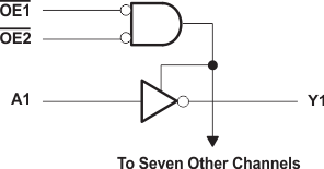
The SNx4AHC540 octal buffers/drivers are ideal for driving bus lines or buffer memory address registers. These devices feature inputs and outputs on opposite sides of the package to facilitate printed circuit board layout.
The 3-state control gate is a two-input AND gate with active-low inputs. If either output-enable (OE1 or OE2) input is high, all corresponding outputs are in the high-impedance state. The outputs provide inverted data when they are not in the high-impedance state.
OE should be tied to VCC through a pullup resistor to ensure the high-impedance state during power up or power down. The minimum value of the resistor is determined by the current-sinking capability of the driver.
8.3 Feature Description
SNx4AHC540 device has a wide operating voltage range and operates from 2 V to 5.5 V. The inputs accept voltages up to 5.5 V, which allows for down translation. Slow input edges and low drive will minimize output overshoots and undershoots.
8.4 Device Functional Modes
Table 1 shows the device functions for each buffer and driver.
