ZHCSAC4B October 2012 – November 2017 SN65HVD82
PRODUCTION DATA.
8 Detailed Description
8.1 Overview
The SN65HVD82 device is a half-duplex RS-485 transceiver suitable for data transmission at rates up to 250 kbps over controlled-impedance transmission media (such as twisted-pair cabling). The device features a high level of internal transient protection, making it able to withstand up ESD strikes up to 12 kV (per IEC 61000-4-2) and EFT transients up to 4 kV (per IEC 61000-4-4) without incurring damage. Up to 256 units of SN65HVD82 may share a common RS-485 bus due to the device’s low bus input currents. The device also features a low standby current consumption of 400 nA (typical).
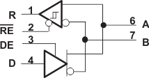
8.2 Functional Block Diagram
 Figure 13. Logic Diagram (Positive Logic)
8.3 Feature Description
8.3.1 Receiver Failsafe
The differential receiver is failsafe to invalid bus states caused by:
- open bus conditions such as a disconnected connector
- shorted bus conditions such as cable damage shorting the twisted-pair together, or
- idle bus conditions that occur when no driver on the bus is actively driving
Receiver failsafe is accomplished by offsetting the receiver thresholds so that the “input indeterminate” range does not include zero volts differential. In order to comply with the RS-422 and RS-485 standards, the receiver output must output a High when the differential input VID is more positive than 200 mV, and must output a Low when the VID is more negative than –200 mV. The receiver parameters which determine the failsafe performance are VIT+ and VIT– and VHYS. As seen in the Electrical Characteristics table, differential signals more negative than
–200 mV will always cause a Low receiver output. Similarly, differential signals more positive than 200 mV will always cause a High receiver output.
When the differential input signal is close to zero, it will still be above the VIT+ threshold, and the receiver output will be High. Only when the differential input is more negative than VIT– will the receiver output transition to a Low state. So the noise immunity of the receiver inputs during a bus fault condition includes the receiver hysteresis value VHYS (the separation between VIT+ and VIT– ) as well as the value of VIT+.
Signals which transition from positive to negative (or from negative to positive) will transition only once, ensuring no spurious bits.
8.3.2 Low-Power Standby Mode
When both the driver and receiver are disabled (DE transitions to a low state and RE transitions to a high state) the device enters standby mode. If the enable inputs are in this state for a brief time (e.g. less than 100 ns), the device does not enter standby mode. This prevents inadvertently entering standby mode during driver/receiver enabling. Only when the enable inputs are held in this state a sufficient duration (e.g. for 300 ns or more), the device is assured to be in standby mode. In this low-power standby mode, most internal circuitry is powered down, and the steady-state supply current is typically less than 400 nA. When either the driver or the receiver is re-enabled, the internal circuitry becomes active.
8.4 Device Functional Modes
Table 1. Driver Function Table
| INPUT | ENABLE | OUTPUTS | ||
|---|---|---|---|---|
| D | DE | A | B | |
| H | H | H | L | Actively drive bus High |
| L | H | L | H | Actively drive bus Low |
| X | L | Z | Z | Driver disabled |
| X | OPEN | Z | Z | Driver disabled by default |
| OPEN | H | H | L | Actively drive bus High by default |
Table 2. Receiver Function Table
| DIFFERENTIAL INPUT | ENABLE | OUTPUT | |
|---|---|---|---|
| VID = VA – VB | RE | R | |
| VIT+ < VID | L | H | Receive valid bus High |
| VIT– < VID < VIT+ | L | ? | Indeterminate bus state |
| VID < VIT– | L | L | Receive valid bus Low |
| X | H | Z | Receiver disabled |
| X | OPEN | Z | Receiver disabled by default |
| Open-circuit bus | L | H | Fail-safe high output |
| Short-circuit bus | L | H | Fail-safe high output |
| Idle (terminated) bus | L | H | Fail-safe high output |
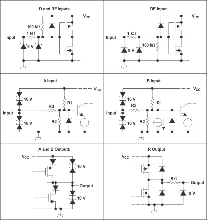
 Figure 14. Equivalent Input and Output Schematic Diagrams