SLLS753E February 2007 – September 2016 SN65HVD1040-Q1
PRODUCTION DATA.
- 1 Features
- 2 Applications
- 3 Description
- 4 Revision History
- 5 Description (continued)
- 6 Pin Configuration and Functions
-
7 Specifications
- 7.1 Absolute Maximum Ratings
- 7.2 ESD Ratings
- 7.3 Recommended Operating Conditions
- 7.4 Thermal Information
- 7.5 Electrical Characteristics: Supply Current
- 7.6 Electrical Characteristics: Driver
- 7.7 Electrical Characteristics: Receiver
- 7.8 Switching Characteristics: Device
- 7.9 Switching Characteristics: Driver
- 7.10 Switching Characteristics: Receiver
- 7.11 STB Pin Characteristics
- 7.12 SPLIT Pin Characteristics
- 7.13 Typical Characteristics
- 8 Parameter Measurement Information
- 9 Detailed Description
- 10Application and Implementation
- 11Power Supply Recommendations
- 12Layout
- 13Device and Documentation Support
- 14Mechanical, Packaging, and Orderable Information
1 Features
- Qualified for Automotive Applications
- AEC-Q100 Test Guidance With the Following:
- Device Temperature Grade 1: –40°C to 125°C Ambient Operating Temperature
- Device HBM ESD Classification Level:
- Level 3A for All Pins Except 1, 5, 6, and 7
- Level 3B for Pins 1, 5, 6, and 7
- Device CDM ESD Classification Level C6
- Device MM ESD Classification Level M3
- Customer-Specific Configuration Control Can Be Supported Along With Major-Change Approval
- Improved Drop-In Replacement for TJA1040
- Meets or Exceeds the Requirements of ISO 11898-5
- GIFT/ICT Compliant
- ESD Protection up to ±8 kV (Human-Body Model) on Bus Pins
- Low-Current Standby Mode With Bus Wakeup, <12 µA Maximum
- High Electromagnetic Immunity (EMI)
- Low Electromagnetic Emissions (EME)
- Bus-Fault Protection of –27 V to 40 V
- Dominant Time-Out Function
- Thermal Shutdown Protection
- Power-Up or Down Glitch-Free Bus Inputs and Outputs
- High Input Impedance With Low VCC
- Monotonic Outputs During Power Cycling
SPACE
2 Applications
- GMW3122 Dual-Wire CAN Physical Layer
- SAE J2284 High-Speed CAN for Automotive Applications
- SAE J1939 Standard Data Bus Interface
- ISO 11783 Standard Data Bus Interface
- NMEA 2000 Standard Data Bus Interface
- Industrial Automation
- DeviceNet™ Data Buses (Vendor ID #806)
3 Description
The SN65HVD1040-Q1 device meets or exceeds the specifications of the ISO 11898 standard for use in applications employing a Controller Area Network (CAN). The device is qualified for use in automotive applications.
As a CAN transceiver, this device provides differential transmit capability to the bus and differential receive capability to a CAN controller at signaling rates up to 1 megabit per second (Mbps). The signaling rate of a line is the number of voltage transitions that are made per second, expressed in the units bps (bits per second).
Device Information(1)
| PART NUMBER | PACKAGE | BODY SIZE (NOM) |
|---|---|---|
| SN65HVD1040-Q1 | SOIC (8) | 4.90 mm × 3.91 mm |
- For all available packages, see the orderable addendum at the end of the data sheet.
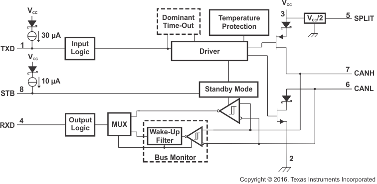
Functional Block Diagram
