SCLS240J October 1995 – December 2014 SN54AHC374 , SN74AHC374
PRODUCTION DATA.
- 1 Features
- 2 Applications
- 3 Description
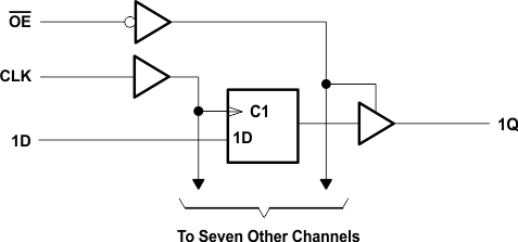
- 4 Simplified Schematic
- 5 Revision History
- 6 Pin Configuration and Functions
-
7 Specifications
- 7.1 Absolute Maximum Ratings
- 7.2 ESD Ratings
- 7.3 Recommended Operating Conditions
- 7.4 Thermal Information
- 7.5 Electrical Characteristics
- 7.6 Timing Requirements, VCC = 3.3 V ± 0.3 V
- 7.7 Timing Requirements, VCC = 5 V ± 0.5 V
- 7.8 Switching Characteristics, VCC = 3.3 V ± 0.3 V
- 7.9 Switching Characteristics, VCC = 5 V ± 0.5 V
- 7.10 Noise Characteristics
- 7.11 Operating Characteristics
- 7.12 Typical Characteristics
- 8 Parameter Measurement Information
- 9 Detailed Description
- 10Application and Implementation
- 11Power Supply Recommendations
- 12Layout
- 13Device and Documentation Support
- 14Mechanical, Packaging, and Orderable Information
封装选项
请参考 PDF 数据表获取器件具体的封装图。
机械数据 (封装 | 引脚)
- W|20
- J|20
- FK|20
散热焊盘机械数据 (封装 | 引脚)
订购信息
9 Detailed Description
9.1 Overview
The SNx4AHC374 devices are octal edge-triggered D-type flip-flops that feature 3-state outputs designed specifically for driving highly capacitive or relatively low-impedance loads. These devices are particularly suitable for implementing buffer registers, I/O ports, bidirectional bus drivers, and working registers.
On the positive transition of the clock (CLK) input, the Q outputs are set to the logic levels of the data (D) inputs.
A buffered output-enable (OE) input can be used to place the eight outputs in either a normal logic state (high or low) or the high-impedance state. In the high-impedance state, the outputs neither load nor drive the bus lines significantly. The high-impedance state and the increased drive provide the capability to drive bus lines without interface or pull-up components.
9.2 Functional Block Diagram
9.3 Feature Description
- Wide operating voltage range
- Operates from 2 V to 5.5 V
- Allows down-voltage translation
- Inputs accept voltages to 5.5 V
- Slow edges reduce output ringing
9.4 Device Functional Modes
Table 1. Function Table
(Each Flip-Flop)
| INPUTS | OUTPUT Q |
||
|---|---|---|---|
| OE | CLK | D | |
| L | ↑ | H | H |
| L | ↑ | L | L |
| L | H or L | X | Q0 |
| H | X | X | Z |