ZHCSD28C November 2012 – December 2014 RF430FRL152H , RF430FRL153H , RF430FRL154H
PRODUCTION DATA.
- 1器件概述
- 2修订历史记录
- 3Device Comparison
- 4Terminal Configuration and Functions
-
5Specifications
- 5.1 Absolute Maximum Ratings
- 5.2 ESD Ratings
- 5.3 Recommended Operating Conditions
- 5.4 Recommended Operating Conditions, Resonant Circuit
- 5.5 Active Mode Supply Current Into VDDB Excluding External Current
- 5.6 Low-Power Mode Supply Current (Into VDDB) Excluding External Current
- 5.7 Digital I/Os (P1, RST/NMI)
- 5.8 High-Frequency Oscillator (4 MHz), HFOSC
- 5.9 Low-Frequency Oscillator (256 kHz), LFOSC
- 5.10 Wake-Up From Low-Power Modes
- 5.11 Timer_A
- 5.12 eUSCI (SPI Master Mode) Recommended Operating Conditions
- 5.13 eUSCI (SPI Master Mode)
- 5.14 eUSCI (SPI Slave Mode)
- 5.15 eUSCI (I2C Mode)
- 5.16 FRAM
- 5.17 JTAG
- 5.18 RFPMM, Power Supply Switch
- 5.19 RFPMM, Bandgap Reference
- 5.20 RFPMM, Voltage Doubler
- 5.21 RFPMM, Voltage Supervision
- 5.22 SD14, Performance
- 5.23 SVSS Generator
- 5.24 Thermistor Bias Generator
- 5.25 Temperature Sensor
- 5.26 RF13M, Power Supply and Recommended Operating Conditions
- 5.27 RF13M, ISO/IEC 15693 ASK Demodulator
- 5.28 RF13M, ISO/IEC 15693 Compliant Load Modulator
-
6Detailed Description
- 6.1 CPU
- 6.2 Instruction Set
- 6.3 Operating Modes
- 6.4 Interrupt Vector Addresses
- 6.5 Memory
- 6.6
Peripherals
- 6.6.1 Digital I/O, (P1.x)
- 6.6.2 Versatile I/O Port P1
- 6.6.3 Oscillator and System Clock
- 6.6.4 Compact System Module (C-SYS_A)
- 6.6.5 Watchdog Timer (WDT_A)
- 6.6.6 Reset, NMI, SVMOUT System
- 6.6.7 Timer_A (Timer0_A3)
- 6.6.8 Enhanced Universal Serial Communication Interface (eUSCI_B0)
- 6.6.9 ISO/IEC 15693 Analog Front End (RF13M)
- 6.6.10 ISO/IEC 15693 Decoder/Encoder (RF13M)
- 6.6.11 CRC16 Module (CRC16)
- 6.6.12 14-Bit Sigma-Delta ADC (SD14)
- 6.6.13 Programmable Gain Amplifier (SD14)
- 6.6.14 Peripheral Register Map
- 6.7 Port Schematics
- 6.8 Device Descriptors (TLV)
- 7Applications, Implementation, and Layout
- 8器件和文档支持
- 9机械封装和可订购信息
封装选项
机械数据 (封装 | 引脚)
- RGE|24
散热焊盘机械数据 (封装 | 引脚)
- RGE|24
订购信息
4 Terminal Configuration and Functions
4.1 Pin Diagram
Figure 4-1 shows the pin assignments on the 24-pin RGE package.
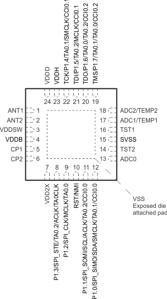 Figure 4-1 24-Pin RGE Package (Top View)
4.2 Signal Descriptions
Table 4-1 describes the signals.
Table 4-1 Signal Descriptions
| TERMINAL | I/O(1) | DESCRIPTION | |
|---|---|---|---|
| NAME | NO. | ||
| ANT1 | 1 | I | Antenna input 1 |
| ANT2 | 2 | I | Antenna input 2 |
| VDDSW | 3 | Switched supply voltage | |
| VDDB | 4 | Battery supply voltage | |
| CP1 | 5 | Charge pump flying cap terminal 1 | |
| CP2 | 6 | Charge pump flying cap terminal 2 | |
| VDD2X | 7 | Voltage doubler output | |
|
P1.3 SPI_STE TA0.2 ACLK TA0CLK |
8 | I/O |
General-purpose digital I/O SPI slave transmit enable Timer_A TA0 OUT2 output ACLK output (divided by 1, 2, 4, 8, 16, or 32) Timer_A TA0 clock signal TA0CLK input |
|
P1.2 SPI_CLK MCLK TA0.0 |
9 | I/O |
General-purpose digital I/O SPI clock MCLK output Timer_A TA0 OUT0 output |
| RST/NMI | 10 | I |
Reset input active low Non-maskable interrupt input |
|
P1.1 SPI_SOMI SCL ACLK TA0.2 CCI0.0 |
11 | I/O |
General-purpose digital I/O SPI slave out master in I2C clock ACLK output (divided by 1, 2, 4, or 8 ) Timer_A TA0 OUT2 output Timer_A TA0 CCR0 capture: CCI0B input, compare |
|
P1.0 SPI_SIMO SDA SMCLK TA0.1 CCI0.0 |
12 | I/O |
General-purpose digital I/O SPI slave in master out I2C data SMCLK output Timer0_A3 OUT1 output Timer_A TA0 CCR0 capture: CCI0A input, compare |
| ADC0 | 13 | I | ADC input pin 0 |
| TST2 | 14 | Internal; connect to GND | |
| SVSS | 15 | Sensor reference potential | |
| TST1 | 16 | Internal; connect to GND | |
| ADC1 / TEMP1 | 17 | ADC input pin 1 / Resistive bias pin 1 | |
| ADC2 / TEMP2 | 18 | ADC input pin 2 / Resistive bias pin 2 | |
|
TMS P1.7 TA0.1 TA0.0 CCI0.2 |
19 | I/O |
JTAG test mode select General-purpose digital I/O Timer_A TA0 OUT1 output Timer_A TA0 OUT0 output Timer_A TA0 CCR2 capture: CCI2B input, compare |
|
TDO P1.6 TA0.0 TA0.2 CCI0.2 |
20 | I/O |
JTAG test data output General-purpose digital I/O Timer_A TA0 OUT0 output Timer_A TA0 OUT2 output Timer_A TA0 CCR2 capture: CCI2A input, compare |
|
TDI P1.5 TA0.2 MCLK CCI0.1 |
21 | I/O |
JTAG test data input General-purpose digital I/O Timer_A TA0 OUT2 output MCLK output Timer_A TA0 CCR1 capture: CCI1B input, compare |
|
TCK P1.4 TA0.1 SMCLK CCI0.1 CLKIN |
22 | I/O |
JTAG test clock General-purpose digital I/O Timer_A TA0 OUT1 output SMCLK output Timer_A TA0 CCR1 capture: CCI1A input, compare External clock input pin |
| VDDH | 23 | O | Rectified voltage from RF-AFE |
| VDDD | 24 | Digital supply voltage | |
| VSS | Pad | Ground reference, bonded to exposed pad(2) | |
4.3 Pin Multiplexing
The GPIO port pins are multiplexed with other functions including analog peripherals and serial communication modules. The pin functions are selected by a combination of register values and device modes. For schematics of the port pins and details of the multiplexing for each, refer to Section 6.7.
4.4 Connections for Unused Pins
The correct termination of all unused pins is listed in Table 4-2.
Table 4-2 Connection of Unused Pins
| Pin | Potential | Comment |
|---|---|---|
| TDI/TMS/TCK | Open | When used for JTAG function |
| RST/NMI | VCC or VSS | 10-nF capacitor to GND/VSS |
| Px.0 to Px.7 | Open | Set to port function, output direction |
| TDO | Open | Convention: leave TDO terminal as JTAG function |