ZHCSE57A September 2015 – November 2015 RF430CL331H
PRODUCTION DATA.
- 1器件概述
- 2修订历史记录
- 3Terminal Configuration and Functions
-
4Specifications
- 4.1 Absolute Maximum Ratings
- 4.2 ESD Ratings
- 4.3 Recommended Operating Conditions
- 4.4 Recommended Operating Conditions, Resonant Circuit
- 4.5 Supply Currents
- 4.6 Electrical Characteristics, Digital Inputs
- 4.7 Electrical Characteristics, Digital Outputs
- 4.8 Thermal Characteristics
- 4.9 Timing and Switching Characteristics
-
5Detailed Description
- 5.1 Overview
- 5.2 Functional Block Diagram
- 5.3 Terms and Acronyms
- 5.4 Serial Communication Interface
- 5.5 Communication Protocol
- 5.6 I2C Protocol
- 5.7 NFC Type 4B Tag Platform
- 5.8 NDEF Structure
- 5.9
Typical Operation
- 5.9.1 NDEF or Capability Container Select Procedure
- 5.9.2 NDEF or Capability Container Read Binary Procedure
- 5.9.3 NDEF or Capability Container Read Procedure (Prefetch Feature)
- 5.9.4 NDEF or Capability Container Write Procedure (Blocking)
- 5.9.5 NDEF or Capability Container Write Procedure (Nonblocking)
- 5.10 RF Command Response Timing Limits
- 5.11
Registers
- 5.11.1 General Control Register
- 5.11.2 Status Register
- 5.11.3 Interrupt Registers
- 5.11.4 CRC Registers
- 5.11.5 Communication Watchdog Register
- 5.11.6 Version Register
- 5.11.7 NDEF File Identifier Register
- 5.11.8 Host Response Register
- 5.11.9 NDEF Block Length Register
- 5.11.10 NDEF File Offset Register
- 5.11.11 Buffer Start Register
- 5.11.12 SWTX Register
- 5.11.13 Custom Status Word Response Register
- 5.12 Identification
- 6Applications, Implementation, and Layout
- 7器件和文档支持
- 8机械、封装和可订购信息
封装选项
机械数据 (封装 | 引脚)
散热焊盘机械数据 (封装 | 引脚)
- RGT|16
订购信息
3 Terminal Configuration and Functions
3.1 Pin Diagrams
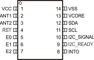
Figure 3-1 shows the pinout for the 14-pin PW package.
 Figure 3-1 14-Pin PW Package (Top View)
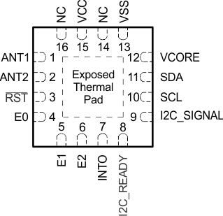
Figure 3-2 shows the pinout for the 16-pin RGT package.
 Figure 3-2 16-Pin RGT Package (Top View)
3.2 Pin Attributes
Table 3-1 Pin Attributes
| PIN NUMBER | SIGNAL NAME | SIGNAL TYPE (1) | BUFFER TYPE (2) | POWER SOURCE | RESET STATE (3) | |
|---|---|---|---|---|---|---|
| PW | RGT | |||||
| 1 | 15 | VCC | PWR | Power | VCC | N/A |
| 2 | 1 | ANT1 | RF | Analog | – | N/A |
| 3 | 2 | ANT2 | RF | Analog | – | N/A |
| 4 | 3 | RST | I | LVCMOS | VCC | PU |
| 5 | 4 | E0 | I | LVCMOS | VCC | OFF |
| 6 | 5 | E1 | I | LVCMOS | VCC | OFF |
| 7 | 6 | E2 | I | LVCMOS | VCC | OFF |
| 8 | 7 | INTO | O | LVCMOS | VCC | OFF |
| 9 | 8 | I2C_READY | O | LVCMOS | VCC | DRIVE1 |
| 10 | 9 | I2C_SIGNAL | O | LVCMOS | VCC | DRIVE1 |
| 11 | 10 | SCL | I/O | LVCMOS | VCC | OFF |
| 12 | 11 | SDA | I/O | LVCMOS | VCC | OFF |
| 13 | 12 | VCORE | PWR | Power | VCC | N/A |
| 14 | 13 | VSS | PWR | Power | VCC | N/A |
| – | 14 | NC | – | – | – | – |
| – | 16 | NC | – | – | – | – |
(1) Signal Types: I = Input, O = Output, I/O = Input or Output, PWR = Power, RF = Radio frequency
(2) Buffer Types: See Table 3-3 for details.
(3) Reset States:
OFF = High-impedance input with pullup or pulldown disabled (if available)
PD = High-impedance input with pulldown enabled
PU = High-impedance input with pullup enabled
DRIVE0 = Drive output low
DRIVE1 = Drive output high
N/A = Not applicable
OFF = High-impedance input with pullup or pulldown disabled (if available)
PD = High-impedance input with pulldown enabled
PU = High-impedance input with pullup enabled
DRIVE0 = Drive output low
DRIVE1 = Drive output high
N/A = Not applicable
3.3 Signal Descriptions
Table 3-2 describes the signals.
Table 3-2 Signal Descriptions
| FUNCTION | SIGNAL NAME | PIN NUMBER | I/O (1) | DESCRIPTION | |
|---|---|---|---|---|---|
| PW | RGT | ||||
| Power | VCC | 1 | 15 | PWR | 3.3-V power supply |
| VCORE | 13 | 12 | PWR | Regulated core supply voltage | |
| VSS | 14 | 13 | PWR | Ground supply | |
| RF | ANT1 | 2 | 1 | RF | Antenna input 1 |
| ANT2 | 3 | 2 | RF | Antenna input 2 | |
| Serial communication | E0 | 5 | 4 | I | I2C address select 0 |
| E1 | 6 | 5 | I | I2C address select 1 | |
| E2 | 7 | 6 | I | I2C address select 2 | |
| I2C_READY | 9 | 8 | O | High indicates that I2C communication can be started. Low indicates that I2C communication must not be started. | |
| I2C_SIGNAL | 10 | 9 | O | Low indicates that a wait time extension command is automatically being sent. I2C communication does not have to be stopped. | |
| SCL | 11 | 10 | I/O | I2C clock | |
| SDA | 12 | 11 | I/O | I2C data | |
| System | INTO | 8 | 7 | O | Interrupt output |
| RST | 4 | 3 | I | Reset input (active low) (2) | |
| No connect | NC | – | 14 16 |
– | Leave open, no connection |
(1) I = Input, O = Output, PWR = Power, RF = RF antenna
(2) With integrated pullup
3.4 Pin Multiplexing
None of the pins on this device are multiplexed.
Table 3-3 Buffer Type
| BUFFER TYPE (STANDARD) | NOMINAL VOLTAGE | HYSTERESIS | PU OR PD | NOMINAL PU OR PD STRENGTH (µA) | OUTPUT DRIVE STRENGTH (mA) | OTHER CHARACTERISTICS |
|---|---|---|---|---|---|---|
| LVCMOS | 3.3 V | Y | N/A | See Section 4.6, Electrical Characteristics, Digital Inputs | See Section 4.7, Electrical Characteristics, Digital Outputs | |
| Analog, RF | 3.3 V | N | N/A | N/A | N/A | See analog modules in Section 4, Specifications, for details |
| Power | 3.3 V | Y with SVS on | N/A | N/A | N/A |
3.5 Connections for Unused Pins
Leave no connect (NC) pins unconnected.
Leave unused outputs unconnected.
Drive or pull unused inputs high or low.