SBOS456H September 2008 – February 2015 REF5020A-Q1 , REF5025A-Q1 , REF5030A-Q1 , REF5040A-Q1 , REF5045A-Q1 , REF5050A-Q1
PRODUCTION DATA.
- 1 Features
- 2 Applications
- 3 Description
- 4 Simplified Schematic
- 5 Revision History
- 6 Pin Configuration and Functions
- 7 Specifications
- 8 Detailed Description
- 9 Application and Implementation
- 10Power Supply Recommendations
- 11Layout
- 12Device and Documentation Support
- 13Mechanical, Packaging, and Orderable Information
11 Layout
11.1 Layout Guidelines
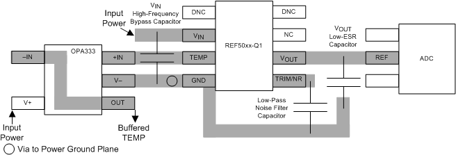
Refer to Figure 33 and use the following guidelines for proper layout design:
- Connect low-ESR, 0.1-μF ceramic bypass capacitors at the VIN and VOUT pins.
- Decouple other active devices in the system per the device specifications.
- Use a solid ground plane to help distribute heat and reduce electromagnetic-interference (EMI) noise pickup.
- Place the external components as close to the device as possible. This configuration prevents parasitic errors (such as the Seebeck effect) from occurring.
- Minimize trace length between the reference and bias connections to the end device to reduce noise pickup.
- Do not run sensitive analog traces in parallel with digital traces. Avoid crossing digital and analog traces if possible and only make perpendicular crossings when absolutely necessary.
11.2 Layout Example
 Figure 33. REF50xxA-Q1 Layout Example