SBOS392H August   2007  – August 2019 REF3312 , REF3318 , REF3320 , REF3325 , REF3330 , REF3333

PRODUCTION DATA.  

  1. Features
  2. Applications
  3. Description
    1.     Device Images
      1.      REF3312 in a Single-Supply Signal Chain
      2.      Dropout Voltage vs Load Current
  4. Revision History
  5. Device Comparison
  6. Pin Configuration and Functions
    1. Table 1. Pin Functions
  7. Specifications
    1. 7.1 Absolute Maximum Ratings
    2. 7.2 ESD Ratings
    3. 7.3 Recommended Operating Conditions
    4. 7.4 Thermal Information
    5. 7.5 Electrical Characteristics
    6. 7.6 Typical Characteristics
  8. Parameter Measurement Information
    1. 8.1 Thermal Hysteresis
  9. Detailed Description
    1. 9.1 Overview
    2. 9.2 Functional Block Diagram
    3. 9.3 Feature Description
      1. 9.3.1 Start-Up Time
      2. 9.3.2 Low Temperature Drift
      3. 9.3.3 Power Dissipation
      4. 9.3.4 Noise Performance
    4. 9.4 Device Functional Modes
  10. 10Applications and Implementation
    1. 10.1 Application Information
    2. 10.2 Typical Applications
      1. 10.2.1 REF3312 in a Bipolar Signal-Chain Configuration
        1. 10.2.1.1 Design Requirements
        2. 10.2.1.2 Detailed Design Procedure
          1. 10.2.1.2.1 Op Amp Level-Shift Design
          2. 10.2.1.2.2 Differential Input Attenuator Design
          3. 10.2.1.2.3 Input Filtering
          4. 10.2.1.2.4 Component Selection
            1. 10.2.1.2.4.1 Voltage References
            2. 10.2.1.2.4.2 Op Amp
          5. 10.2.1.2.5 Input Attenuation and Level Shifting
          6. 10.2.1.2.6 Input Filtering
          7. 10.2.1.2.7 Passive Component Tolerances and Materials
        3. 10.2.1.3 Application Curves
          1. 10.2.1.3.1 DC Performance
          2. 10.2.1.3.2 AC Performance
  11. 11Power-Supply Recommendations
  12. 12Layout
    1. 12.1 Layout Guidelines
    2. 12.2 Layout Example
  13. 13Device and Documentation Support
    1. 13.1 Documentation Support
      1. 13.1.1 Related Documentation
    2. 13.2 Related Links
    3. 13.3 Receiving Notification of Documentation Updates
    4. 13.4 Community Resources
    5. 13.5 Trademarks
    6. 13.6 Electrostatic Discharge Caution
    7. 13.7 Glossary
  14. 14Mechanical, Packaging, and Orderable Information

封装选项

机械数据 (封装 | 引脚)
散热焊盘机械数据 (封装 | 引脚)
订购信息

Overview

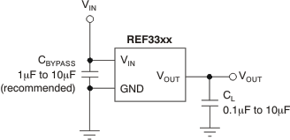
The REF33xx is a family of low-power, precision band-gap voltage references that are specifically designed for extremely low dropout, excellent initial voltage accuracy with a high output current. A simplified block diagram of the REF33xx is shown in the Functional Block Diagram section. Figure 17 shows the typical connections for the REF33xx. A supply bypass capacitor ranging between 1 μF to 10 μF is recommended. The total capacitive load at the output must be between 0.1 μF to 10 μF to ensure output stability.
REF3312 REF3318 REF3320 REF3325 REF3330 REF3333 ai_basic_bos392.gifFigure 17. Basic Connections