SBOS218D December   2001  – May 2016 PGA2311

PRODUCTION DATA.  

  1. Features
  2. Applications
  3. Description
  4. Revision History
  5. Pin Configuration and Functions
  6. Specifications
    1. 6.1 Absolute Maximum Ratings
    2. 6.2 ESD Ratings
    3. 6.3 Recommended Operating Conditions
    4. 6.4 Thermal Information
    5. 6.5 Electrical Characteristics
    6. 6.6 Typical Characteristics
  7. Detailed Description
    1. 7.1 Overview
    2. 7.2 Functional Block Diagram
    3. 7.3 Feature Description
      1. 7.3.1 Analog Inputs and Outputs
      2. 7.3.2 Gain Settings
      3. 7.3.3 Daisy-Chaining Multiple PGA2311 Devices
      4. 7.3.4 Zero-Crossing Detection
      5. 7.3.5 MUTE Function
    4. 7.4 Device Functional Modes
      1. 7.4.1 Power-Up State
    5. 7.5 Programming
  8. Application and Implementation
    1. 8.1 Application Information
    2. 8.2 Typical Application
      1. 8.2.1 Design Requirements
      2. 8.2.2 Detailed Design Procedure
      3. 8.2.3 Application Curve
  9. Power Supply Recommendations
  10. 10Layout
    1. 10.1 Layout Guidelines
    2. 10.2 Layout Example
  11. 11Device and Documentation Support
    1. 11.1 Documentation Support
      1. 11.1.1 Related Documentation
    2. 11.2 Community Resources
    3. 11.3 Trademarks
    4. 11.4 Electrostatic Discharge Caution
    5. 11.5 Glossary
  12. 12Mechanical, Packaging, and Orderable Information

封装选项

机械数据 (封装 | 引脚)
散热焊盘机械数据 (封装 | 引脚)
订购信息

10 Layout

10.1 Layout Guidelines

The ground planes for the digital and analog sections of the PCB must be separate from one another. The planes must be connected at a single point. Figure 15 shows the recommended PCB floor plan for the PGA2311.

The PGA2311 is mounted so that the device straddles the split between the digital and analog ground planes. Pins 1 through 8 are oriented to the digital side of the board and pins 9 through 16 are on the analog side of the board.

10.2 Layout Example
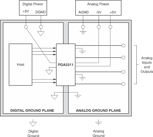
PGA2311 pcb_layout.gif Figure 15. Typical PCB Layout Floor Plan