SLES211C February 2008 – July 2015 PCM1681 , PCM1681-Q1
PRODUCTION DATA.
- 1 Features
- 2 Applications
- 3 Description
- 4 Revision History
- 5 Description (continued)
- 6 Pin Configuration and Functions
- 7 Specifications
-
8 Detailed Description
- 8.1 Overview
- 8.2 Functional Block Diagram
- 8.3 Feature Description
- 8.4 Device Functional Modes
- 8.5 Programming
- 8.6
Register Maps
- 8.6.1 Reserved Registers
- 8.6.2
Register Definitions
- 8.6.2.1 ATx[7:0]: Digital Attenuation Level Setting
- 8.6.2.2 MUTx: Soft Mute Control
- 8.6.2.3 DACx: DAC Operation Control
- 8.6.2.4 FLT: Digital Filter Roll-Off Control
- 8.6.2.5 FMT[3:0]: Audio Interface Data Format
- 8.6.2.6 SRST: Reset
- 8.6.2.7 ZREV: Zero-Flag Polarity Select
- 8.6.2.8 DREV: Output Phase Select
- 8.6.2.9 DMF[1:0]: Sampling Frequency Selection for the De-Emphasis Function
- 8.6.2.10 DMC: Digital De-Emphasis All-Channel Function Control
- 8.6.2.11 REV[8:1]: Output Phase Select per Channel
- 8.6.2.12 OVER: Oversampling Rate Control
- 8.6.2.13 FLTx: Digital Filter Roll-Off Control per DATA Group
- 8.6.2.14 DAMS: Digital Attenuation Mode Select
- 8.6.2.15 AZRO[1:0]: Zero-Flag Channel-Combination Select
- 8.6.2.16 ZERO[8:1]: Zero-Detect Status (Read-Only, I2C Interface Only)
- 9 Application and Implementation
- 10Power Supply Recommendations
- 11Layout
- 12Device and Documentation Support
- 13Mechanical, Packaging, and Orderable Information
封装选项
机械数据 (封装 | 引脚)
- PWP|28
散热焊盘机械数据 (封装 | 引脚)
- PWP|28
订购信息
8 Detailed Description
8.1 Overview
The PCM1681 and PCM1681-Q1 are CMOS monolithic integrated circuits which feature an eight-channel 24-bit audio digital-to-analog converter (DAC) and support circuitry in small 28-lead TSSOP PowerPAD packages. The DACs utilize a Burr-Brown enhanced multilevel delta-sigma (ΔΣ) architecture to achieve excellent signal-to-noise performance and a high tolerance to clock jitter. The system clock can operate anywhere from 128 fs to 1152 fs and with respect to the system clock rate the DAC can oversample anywhere from ×16 to ×128. The PCM1681 and PCM1681-Q1 accept TDM (time-division multiplexed) format in addition to industry-standard audio data formats with 16- to 24-bit audio data width. This includes right justified, I2S, left justified, and DSP formats along with sampling rates up to 200 kHz. The PCM1681 and PCM1681-Q1 provide a sub-set of user-programmable functions through a parallel control port, in addition to a full set of user-programmable functions through a serial control port, SPI, or I2C. This is controlled through the MSEL pin as explained in Table 7. A 5-V analog supply and a 3.3-V digital supply are required. The PCM1681 supports –40°C to 85°C for consumer grade applications and the PCM1681-Q1 supports –40°C to 105°C for automotive audio grade systems.
8.2 Functional Block Diagram
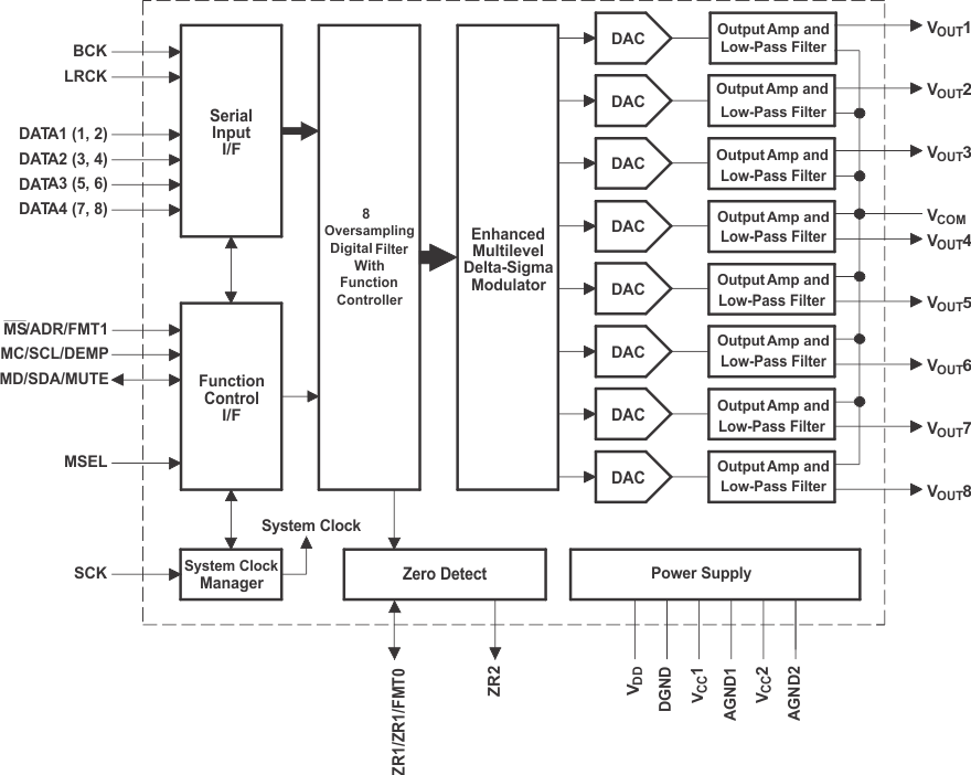
8.3 Feature Description
8.3.1 System Clock Input
The PCM1681 and PCM1681-Q1 require a system clock for operating the digital interpolation filters and multilevel ΔΣ modulators. The system clock is applied at the SCK input (pin 5). Table 1 shows examples of system clock frequencies for common audio sampling rates.
Figure 21 shows the timing requirements for the system clock input. For optimal performance, it is important to use a clock source with low phase jitter and noise. A Texas Instruments PLL170x multi-clock generator is an excellent choice for providing the PCM1681 and PCM1681-Q1 system clock source.
Table 1. System Clock Frequencies for Common Audio Sampling Frequencies
| SAMPLING FREQUENCY | SYSTEM CLOCK FREQUENCY (fSCK), MHz | ||||||
|---|---|---|---|---|---|---|---|
| 128 fS | 192 fS | 256 fS | 384 fS | 512 fS | 768 fS | 1152 fS | |
| 8 kHz | 1.024 | 1.536 | 2.048 | 3.072 | 4.096 | 6.144 | 9.216 |
| 16 kHz | 2.048 | 3.072 | 4.096 | 6.144 | 8.192 | 12.288 | 18.432 |
| 32 kHz | 4.096 | 6.144 | 8.192 | 12.288 | 16.384 | 24.576 | 36.864 |
| 44.1 kHz | 5.6448 | 8.4672 | 11.2896 | 16.9344 | 22.5792 | 33.8688 | —(1) |
| 48 kHz | 6.144 | 9.216 | 12.288 | 18.432 | 24.576 | 36.864 | —(1) |
| 88.2 kHz | 11.2896 | 16.9344 | 22.5792 | 33.8688 | —(1) | —(1) | —(1) |
| 96 kHz | 12.288 | 18.432 | 24.576 | 36.864 | —(1) | —(1) | —(1) |
| 192 kHz | 24.576 | 36.864 | —(1) | —(1) | —(1) | —(1) | —(1) |

Table 2. System Clock Timing
| PARAMETER | MIN | MAX | UNIT | |
|---|---|---|---|---|
| tc(SCK) | System clock cycle time | 25 | ns | |
| tw(SCKH) | System clock pulse duration, HIGH | 10 | ns | |
| tw(SCKL) | System clock pulse duration, LOW | 10 | ns | |
| System clock duty cycle | 40% | 60% | ||
8.3.2 Power-on-Reset Function
The PCM1681 and PCM1681-Q1 include a power-on-reset function. Figure 22 shows the operation of this function. With the system clock active and VDD > 2.2 V (typical, 1.4 V to 2.9 V), the power-on-reset function is enabled. The initialization sequence requires 65,536 system clocks from the time VDD > 2.2 V. VDD must rise up with a ramp-up rate greater than 1V/ms to ensure reliable initialization. After the initialization period, the PCM1681 and PCM1681-Q1 are set to the respective reset default state, as described in the Mode Control Registers section of this data sheet.
During the reset period (65,536 system clocks), the analog output is forced to the common voltage (VCOM), or VCC/2. After the reset period, the internal register is initialized in the next 1/fS period and if SCK, BCK, and LRCK are provided continuously, the PCM1681 and PCM1681-Q1 provide the proper analog output with group delay corresponding to the input data.
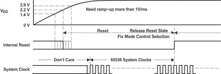 Figure 22. Power-On-Reset Timing
8.3.3 Audio Serial Interface
The audio serial interface for the PCM1681 and PCM1681-Q1 is comprised of a 6-wire synchronous serial port. It includes LRCK (pin 8), BCK (pin 7), and DATA1 (pin 6), DATA2 (pin 11), DATA3 (pin 12), and DATA4 (pin 13). BCK is the serial audio bit clock, and it is used to clock the serial data present on DATA1, DATA2, DATA3, and DATA4 into the audio interface serial shift register. Serial data are clocked into the PCM1681 and PCM1681-Q1 on the rising edge of BCK. LRCK is the serial audio left/right word clock. It is used to latch serial data into the serial audio interface internal registers.
Both LRCK and BCK must be synchronous with the system clock, SCK. Ideally, it is recommended that LRCK and BCK are derived from SCK. LRCK is operated at the sampling frequency, fS. BCK can be operated at 32, 48, or 64 times the sampling frequency for the PCM formats and times at 128 and 256 the sampling frequency for the TDM formats.
Internal operation of the PCM1681 and PCM1681-Q1 is synchronized with LRCK. Accordingly, internal operation is suspended when LRCK is changed or when SCK and/or BCK is interrupted for at least 3-bit clock cycles. If SCK, BCK, and LRCK are provided continuously after this held condition, the internal operation is resynchronized automatically within the following 3/fS period. External resetting is not required.
8.3.4 Audio Data Formats and Timing
The PCM1681 and PCM1681-Q1 support industry-standard audio data formats, including right-justified, I2S, left-justified, and DSP. The PCM1681 and PCM1681-Q1 also support a time-division-multiplexed (TDM) format. The TDM format is supported only at system clocks of 128 fS, 256 fS, and 512 fS. The data formats are shown in Figure 23 and Figure 24. Data formats are selected using the format bits, FMT[3:0], located in control register 9 of the PCM1681 and PCM1681-Q1. The default data format is 16- to 24-bit left-justified. All formats require binary 2s complement, MSB-first audio data. Figure 25 shows a detailed timing diagram for the serial audio interface.
DATA1, DATA2, DATA3, and DATA4 each carry two audio channels, designated as the left and right channels in the right-justified, I2S, left-justified, and DSP formats. The left-channel data always precedes the right-channel data in the serial data stream for all data formats. Table 3 shows the mapping of the digital input data to the analog output pins. DATA1 carries eight audio channels in 256 fS mode TDM fornat, and DATA1 and DATA2 each carry four audio channels in 128 fS mode TDM format.
Table 3. Audio Input Data to Analog Output Mapping
| DATA INPUT | CHANNEL | ANALOG OUTPUT |
|---|---|---|
| DATA1 | Left | VOUT1 |
| Right | VOUT2 | |
| DATA2 | Left | VOUT3 |
| Right | VOUT4 | |
| DATA3 | Left | VOUT5 |
| Right | VOUT6 | |
| DATA4 | Left | VOUT7 |
| Right | VOUT8 |
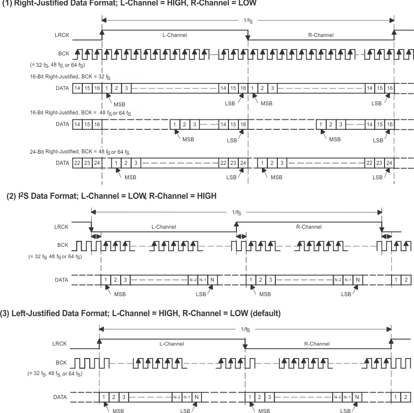 Figure 23. Audio Data Input Formats
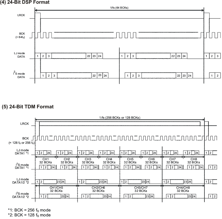 Figure 24. Audio Data Input Formats
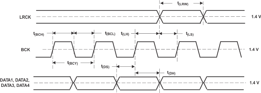 Figure 25. Audio Interface Timing Diagram
Table 4. Audio Interface Timing
| PARAMETER | MIN | MAX | UNIT | |
|---|---|---|---|---|
| t(BCY) | BCK cycle time | 75(1) | ns | |
| t(BCH) | BCK pulse duration HIGH | 35 | ns | |
| t(BCL) | BCK pulse duration LOW | 35 | ns | |
| t(LRW) | LRCK pulse duration HIGH, right-justified, I2S, left-justified | 1/2 fS | 1/2 fS | |
| LRCK pulse duration HIGH, DSP format | t(BCY) | t(BCY) | ||
| LRCK pulse duration HIGH, TDM format | t(BCY) | 1/fS – t(BCY) | ||
| t(LS) | LRCK setup time to BCK rising edge | 10 | ns | |
| t(LH) | LRCK hold time to BCK rising edge | 10 | ns | |
| t(DS) | DATA1, DATA2, DATA3, DATA4 setup time to BCK rising edge | 10 | ns | |
| t(DH) | DATA1, DATA2, DATA3, DATA4 hold time to BCK rising edge | 10 | ns | |
8.3.5 De-Emphasis Filter
The PCM1681 and PCM1681-Q1 include a digital de-emphasis filter for 32 kHz, 44.1 kHz, and 48 kHz sampling frequencies.
8.3.6 Oversampling Rate Control
The PCM1681 and PCM1681-Q1 automatically control the oversampling rate of the ΔΣ DACs according to system clock frequency and oversampling mode. Oversampling mode, narrow or wide, can be selected by the MSEL pin in H/W control mode and the OVER bit of control register 12 in S/W control mode. The oversampling rate is set to 64× oversampling with a 1152 fS, 768 fS, 512 fS system clock, 32× oversampling with a 384 fS, 256 fS system clock, and 16× oversampling with a 192 fS, 128 fS system clock in default, narrow mode, and 128× oversampling with a 1152 fS, 768 fS, 512 fS system clock, 64× oversampling with a 384 fS, 256 fS system clock, and 32× oversampling with a 192 fS, 128 fS system clock in wide mode. Wide mode is recommended for fS ≤ 96 kHz at SCK = 128 fS or 192 fS, fS ≤ 48 kHz at SCK = 256 fS or 384 fS, and fS ≤ 24 kHz at SCK = 512 fS, 768 fS, or 1152 fS.
Table 5. Oversampling Rate Control
| OVERSAMPLING MODE | OVERSAMPLING RATE | ||
|---|---|---|---|
| SCK = 128 fS or 192 fS | SCK = 256 fS or 384 fS | SCK = 512 fS, 768 fS, or 1152 fS | |
| Narrow mode | 16× | 32× | 64× |
| Wide mode | 32× | 64× | 128× |
8.3.7 Zero Flag
The PCM1681 and PCM1681-Q1 have two zero-flag pins, ZR1 (pin 1) and ZR2 (pin 28), which are assigned to the combinations A through D as shown in Table 6. Zero-flag combinations are selected using the zero-flag combination bits, AZRO[1:0], located in control register 13 of the PCM1681 and PCM1681-Q1. If the input data of the L-channel and/or R-channel of all assigned channels remains at a logic-0 level for 1024 sampling periods (LRCK clock periods), ZR1 and ZR2 are set to logic-1 states, or high level. If the input data of any of the assigned channels contains a logic-1 level, ZR1 and ZR2 are set to logic-0 states or low level immediately.
The active polarity of a zero-flag output can be inverted by setting the ZREV bit of control register 10 to 1. The reset default is ZREV = 0, active-high for zero detection.
In parallel hardware control mode, ZR1 is not applicable due to the reassignment of ZR1 as the FMT0 control pin, and the zero-flag output combination is fixed as all 8 channel (DATA1-DATA4) data zero on the ZR2 pin.
Table 6. Zero-Flag Output Combinations
| ZERO-FLAG COMBINATION | ZR1/ZR1/FMT0 (PIN 1) | ZR2 (PIN 28) |
|---|---|---|
| A | DATA1 L-ch | DATA1 R-ch |
| B | DATA1-4 | DATA1-4 |
| C | DATA4 | DATA1-3 |
| D | DATA1 | DATA2-4 |
8.3.8 Mode Control
The PCM1681 and PCM1681-Q1 support three types of interface mode control with three types of oversampling configuration, according to the input state of MSEL (pin 14) as listed in Table 7. The required values of the pull-up and pull-down resistors are 220 kΩ ± 5%.
Table 7. Interface Mode Control
| MSEL | INTERFACE MODE CONTROL |
|---|---|
| Tied with DGND | 2-Wire (I2C) serial control, selectable oversampling configuration |
| Pull-down resistor to DGND | 4-Wire parallel H/W control, narrow mode oversampling configuration |
| Pull-up resistor to VDD | 4-Wire parallel H/W control, wide mode oversampling configuration |
| Tied with VDD | 3-Wire (SPI) serial control, selectable oversampling configuration |
The input state of the MSEL pin is sampled at power-on with the system clock input; therefore, an input change after a reset is ignored until the next power-on. The assignments of the four pins are controlled by the interface mode control setting as listed in Table 8.
Table 8. Interface Mode Control Pin Assignments
| PIN | DEFINITION (Assignment) | ||
|---|---|---|---|
| I2C | SPI | PARALLEL H/W | |
| 4 | SDA (input/output) | MD (input) | MUTE (input) |
| 3 | SCL (input) | MC (input) | DEMP (input) |
| 2 | ADR (input) | MS (input) | FMT1 (input) |
| 1 | ZR1 (output) | ZR1 (output) | FMT0 (input) |
In serial control mode, actual mode control is performed by a register write (and read) through the I2C or SPI compatible serial control port. In parallel H/W control mode, the specific four functions are controlled directly through high-level/low-level control of five specific pins (see Parallel Hardware Control section), and the zero-flag function of ZR1 is not applicable.
8.3.8.1 Parallel Hardware Control
Four functions are controlled by five pins, MSEL, FMT0, FMT1, DEMP, and MUTE in parallel hardware control mode.
| MSEL TERMINATION(1) | DESCRIPTION |
|---|---|
| Pull-down resistor to DGND | Narrow oversampling mode |
| Pull-up resistor to VDD | Wide oversampling mode |
| FMT1(1) | FMT0(1) | DESCRIPTION |
|---|---|---|
| LOW | LOW | 24-bits right-justified format |
| LOW | HIGH | 16 to 24-bits I2S format |
| HIGH | LOW | 16 to 24-bits left-justified format |
| HIGH | HIGH | 24-bits I2S mode TDM format |
| DEMP(1) | DESCRIPTION |
|---|---|
| LOW | De-emphasis off |
| HIGH | 44.1-kHz De-emphasis on |
| MUTE(1) | DESCRIPTION |
|---|---|
| LOW | Mute off (mute disable) |
| HIGH | Mute on (mute enable) |
8.3.8.2 SPI Control Interface
The SPI control interface of the PCM1681 and PCM1681-Q1 is a 3-wire synchronous serial port that operates asynchronously to the serial audio interface. The SPI control interface is used to program the on-chip mode registers. The control interface includes MD (pin 4), MC (pin 3), and MS (pin 2). MD is the serial data input, used to program the mode registers. MC is the control port for the serial bit clock, used to shift in the serial data, and MS is the control port for mode control select, which is used to enable the mode control. The SPI control interface is available when MSEL (pin 14) is tied with VDD and after power-on reset completion.
8.3.8.3 Analog Outputs
The PCM1681 and PCM1681-Q1 include eight independent output channels, VOUT1 through VOUT8. These are unbalanced outputs, each capable of driving 3.75 VPP typical into a 5-kΩ ac load with VCC = 5 V. The internal output amplifiers for VOUT1 through VOUT8 are biased to the dc common voltage, equal to 0.486 VCC.
The output amplifiers include an RC continuous-time filter, which helps to reduce the out-of-band noise energy present at the DAC outputs due to the noise-shaping characteristics of the PCM1681 and PCM1681-Q1 ΔΣ DACs. The frequency response of this filter is shown in Figure 12. By itself, this filter is not enough to attenuate the out-of-band noise to an acceptable level for most applications. An external low-pass filter is required to provide sufficient out-of-band noise rejection. Further discussion of DAC post-filter circuits is provided in the Application and Implementation section of this data sheet.
8.3.8.3.1 VCOM Output
One unbuffered common voltage output pin, VCOM (pin 25), is brought out for decoupling purposes. This pin is nominally biased to the dc common voltage, equal to VCC/2. If this pin is to be used to bias external circuitry, a voltage follower is required for buffering purposes. Figure 26 shows an example of a 5-V single-supply filter circuit using the VCOM pin for external biasing applications.
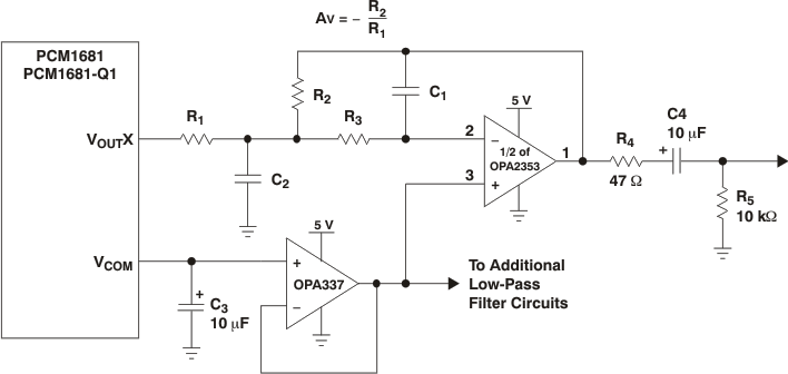
NOINDENT:
Example:R1: 6.2 kΩ
R2: 6.8 kΩ
R3: 430 Ω
C1: 470 pF
C2: 4700 pF
AV: –1.10 (1.45 Vrms Output)
fC: 70 kHz
8.3.8.4 Register Write Operation
All write operations for the serial control port use 16-bit data words. Figure 27 shows the control data word format. The most significant bit is a fixed 0 for the write operation. Seven bits, labeled IDX[6:0], set the register index (or address) for the write operation. The least significant eight bits, D[7:0], contain the data to be written to the register specified by IDX[6:0].
Figure 28 shows the functional timing diagram for writing to the serial control port. MS is held at a logic-1 state until a register needs to be written. To start the register write cycle, MS is set to logic-0. 16 clock cycles are then provided on MC, corresponding to the 16 bits of the control data word on MD. After completion of the 16th clock cycle, MS is set to logic-1 to latch the data into the indexed mode control register.
 Figure 27. Control Data Word Format for MD
 Figure 28. Write Operation Timing
8.3.8.5 Interface Timing Requirements
Figure 29 shows a detailed timing diagram for the serial control interface. Special attention to the setup and hold times is required. Also, t(MSS) and t(MSH), which define the minimum delays between the edges of the MS and MC clocks, require special attention. These timing parameters are critical for proper control port operation.
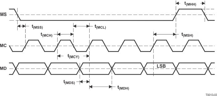 Figure 29. Interface Timing Diagram
Table 9. Interface Timing
| PARAMETER | MIN | UNIT | |
|---|---|---|---|
| t(MCY) | MC cycle time | 100 | ns |
| t(MCL) | MC pulse duration, LOW | 50 | ns |
| t(MCH) | MC pulse duration, HIGH | 50 | ns |
| t(MHH) | MS pulse duration, HIGH | ns(1) | |
| t(MSS) | MS falling edge to MC rising edge | 20 | ns |
| t(MSH) | MS hold time, MC rising edge for LSB to MS rising edge | 20 | ns |
| t(MDH) | MD hold time | 15 | ns |
| t(MDS) | MD setup time | 20 | ns |
8.4 Device Functional Modes
8.4.1 Control Modes
- 3-wire SPI
- I2C
- Hardware Control
8.4.2 Audio Modes
- Right or left justified
- I2S
- TDM
- DSP
8.5 Programming
8.5.1 I2C Interface
The PCM1681 and PCM1681-Q1 support the I2C serial bus and the data transmission protocol for standard mode as a slave device. This protocol is explained in the I2C specification 2.0. The PCM1681 and PCM1681-Q1 do not support a board-to-board interface. The I2C control interface is available when MSEL (pin 14) is tied with DGND and after power-on reset completion.
8.5.1.1 Slave Address
| MSB | LSB |
| 1 | 0 | 0 | 1 | 1 | 0 | ADR | R/W |
The PCM1681 and PCM1681-Q1 have seven bits for the respective slave address. The first six bits (MSBs) of the slave address are factory preset to 1001 10. The next bit of the address byte is the device select bit, which can be user-defined using the ADR terminal. A maximum of two PCM1681s or PCM1681-Q1s can be connected on the same bus at one time. Each PCM1681 or PCM1681-Q1 responds when it receives its own slave address.
8.5.1.2 Packet Protocol
A master device must control packet protocol, which consists of a start condition, slave address, read/write bit, data if writing or acknowledge if reading, and stop condition. The PCM1681 and PCM1681-Q1 support only slave receivers and slave transmitters. The details about DATA for write and read operation are described in the following sections.
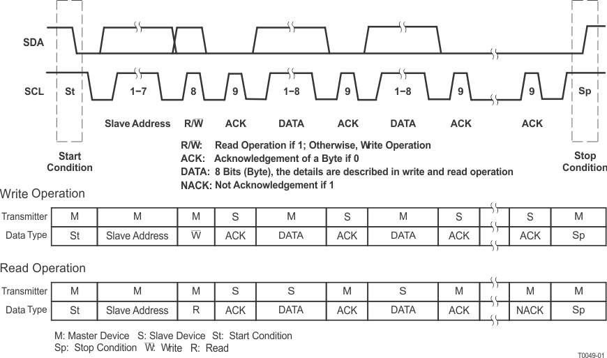 Figure 30. Basic I2C Framework
8.5.1.3 Write Operation
A master can write to any PCM1681 and PCM1681-Q1 registers using a single access. The master sends a PCM1681 or PCM1681-Q1 slave address with a write bit, a register address, and the data. When undefined registers are accessed, the PCM1681 or PCM1681-Q1 sends an acknowledgment, but the write operation does not occur. Figure 31 is a diagram of the write operation.
 Figure 31. Write Operation
8.5.1.4 Read Operation
A master can read any PCM1681 or PCM1681-Q1 register using a single access. The master sends a PCM1681 or PCM1681-Q1 slave address with a read bit after transferring the register address. Then the PCM1681 or PCM1681-Q1 transfers the data in the register specified. Figure 32 is a diagram of the read operation.

NOTE:
The slave address after the repeated start condition must be the same as the previous slave address.8.5.2 Mode Control Registers
8.5.2.1 User-Programmable Mode Controls
The PCM1681 and PCM1681-Q1 include a number of user-programmable functions which are accessed via control registers. The registers are programmed using the serial control interface which is discussed in the Mode Control section of this data sheet. Table 10 lists the available mode control functions, along with the respective reset default conditions and associated register index.
8.6 Register Maps
The mode control register map is shown in Table 11. The MSB of all registers is fixed to 0. Each register also includes an index (or address) indicated by the IDX[6:0] bits.
8.6.1 Reserved Registers
Registers 0 and 15 are reserved for factory use. To ensure proper operation, the user should not write to these registers.
Table 10. User-Programmable Mode Control Functions
| FUNCTION | RESET DEFAULT | REGISTER | BIT |
|---|---|---|---|
| Digital attenuation control, 0 dB to –63 dB in 0.5-dB steps | 0 dB, no attenuation | 1–6, 16, 17 | AT1[7:0], AT2[7:0], AT3[7:0], AT4[7:0], AT5[7:0], AT6[7:0], AT7[7:0], AT8[7:0] |
| Soft mute control | Mute disabled | 7, 18 | MUT[8:1], MUT[8:7] |
| DAC1–DAC8 operation control | DAC1–DAC8 enabled | 8, 19 | DAC[8:1], DAC[8:7] |
| Audio data format control | 16- to 24-bit, left-justified | 9 | FMT[3:0] |
| Digital filter roll-off control | Sharp roll-off | 9 | FLT |
| De-emphasis all-channel function control | De-emphasis of all channels disabled | 10 | DMC |
| De-emphasis all-channel sample rate selection | 44.1 kHz | 10 | DMF[1:0] |
| Output phase select | Normal phase | 10 | DREV |
| Zero-flag polarity select | High | 10 | ZREV |
| Software reset control | Reset disabled | 10 | SRST |
| Output phase select per channel | Reverse phase | 11 | REV[8:1] |
| Oversampling rate control | Narrow (×64, ×32, ×16) mode | 12 | OVER |
| Digital filter roll-off control per DATA group | Slow roll-off | 12 | FLT[4:1] |
| Zero-flag combination select | ZR1: DATA1 Lch ZR2: DATA1 Rch |
13 | AZRO[1:0] |
| Digital attenuation mode select | 0 to –63 dB, 0.5-dB step | 13 | DAMS |
| Zero-detect status (read-only, I2C interface only) |
N/A | 14 | ZERO[8:1] |
Table 11. Mode Control Register Map
| IDX (B8–B14) | REGISTER | B15 | B14 | B13 | B12 | B11 | B10 | B9 | B8 | B7 | B6 | B5 | B4 | B3 | B2 | B1 | B0 |
|---|---|---|---|---|---|---|---|---|---|---|---|---|---|---|---|---|---|
| 00h | 0 | 0 | IDX6 | IDX5 | IDX4 | IDX3 | IDX2 | IDX1 | IDX0 | N/A(1) | N/A(1) | N/A(1) | N/A(1) | N/A(1) | N/A(1) | N/A(1) | N/A(1) |
| 01h | 1 | 0 | IDX6 | IDX5 | IDX4 | IDX3 | IDX2 | IDX1 | IDX0 | AT17 | AT16 | AT15 | AT14 | AT13 | AT12 | AT11 | AT10 |
| 02h | 2 | 0 | IDX6 | IDX5 | IDX4 | IDX3 | IDX2 | IDX1 | IDX0 | AT27 | AT26 | AT25 | AT24 | AT23 | AT22 | AT21 | AT20 |
| 03h | 3 | 0 | IDX6 | IDX5 | IDX4 | IDX3 | IDX2 | IDX1 | IDX0 | AT37 | AT36 | AT35 | AT34 | AT33 | AT32 | AT31 | AT30 |
| 04h | 4 | 0 | IDX6 | IDX5 | IDX4 | IDX3 | IDX2 | IDX1 | IDX0 | AT47 | AT46 | AT45 | AT44 | AT43 | AT42 | AT41 | AT40 |
| 05h | 5 | 0 | IDX6 | IDX5 | IDX4 | IDX3 | IDX2 | IDX1 | IDX0 | AT57 | AT56 | AT55 | AT54 | AT53 | AT52 | AT51 | AT50 |
| 06h | 6 | 0 | IDX6 | IDX5 | IDX4 | IDX3 | IDX2 | IDX1 | IDX0 | AT67 | AT66 | AT65 | AT64 | AT63 | AT62 | AT61 | AT60 |
| 07h | 7 | 0 | IDX6 | IDX5 | IDX4 | IDX3 | IDX2 | IDX1 | IDX0 | MUT8 | MUT7 | MUT6 | MUT5 | MUT4 | MUT3 | MUT2 | MUT1 |
| 08h | 8 | 0 | IDX6 | IDX5 | IDX4 | IDX3 | IDX2 | IDX1 | IDX0 | DAC8 | DAC7 | DAC6 | DAC5 | DAC4 | DAC3 | DAC2 | DAC1 |
| 09h | 9 | 0 | IDX6 | IDX5 | IDX4 | IDX3 | IDX2 | IDX1 | IDX0 | RSV(2) | RSV(2) | FLT | RSV(2) | FMT3 | FMT2 | FMT1 | FMT0 |
| 0Ah | 10 | 0 | IDX6 | IDX5 | IDX4 | IDX3 | IDX2 | IDX1 | IDX0 | SRST | ZREV | DREV | DMF1 | DMF0 | RSV(2) | RSV(2) | DMC |
| 0Bh | 11 | 0 | IDX6 | IDX5 | IDX4 | IDX3 | IDX2 | IDX1 | IDX0 | REV8 | REV7 | REV6 | REV5 | REV4 | REV3 | REV2 | REV1 |
| 0Ch | 12 | 0 | IDX6 | IDX5 | IDX4 | IDX3 | IDX2 | IDX1 | IDX0 | OVER | RSV(2) | RSV(2) | RSV(2) | FLT4 | FLT3 | FLT2 | FLT1 |
| 0Dh | 13 | 0 | IDX6 | IDX5 | IDX4 | IDX3 | IDX2 | IDX1 | IDX0 | DAMS | AZRO1 | AZRO0 | RSV(2) | RSV(2) | RSV(2) | RSV(2) | RSV(2) |
| 0Eh | 14 | 0 | IDX6 | IDX5 | IDX4 | IDX3 | IDX2 | IDX1 | IDX0 | ZERO8 | ZERO7 | ZERO6 | ZERO5 | ZERO4 | ZERO3 | ZERO2 | ZERO1 |
| 10h | 16 | 0 | IDX6 | IDX5 | IDX4 | IDX3 | IDX2 | IDX1 | IDX0 | AT77 | AT76 | AT75 | AT74 | AT73 | AT72 | AT71 | AT70 |
| 11h | 17 | 0 | IDX6 | IDX5 | IDX4 | IDX3 | IDX2 | IDX1 | IDX0 | AT87 | AT86 | AT85 | AT84 | AT83 | AT82 | AT81 | AT80 |
| 12h | 18 | 0 | IDX6 | IDX5 | IDX4 | IDX3 | IDX2 | IDX1 | IDX0 | RSV(2) | RSV(2) | RSV(2) | RSV(2) | RSV(2) | RSV(2) | MUT8 | MUT7 |
| 13h | 19 | 0 | IDX6 | IDX5 | IDX4 | IDX3 | IDX2 | IDX1 | IDX0 | RSV(2) | RSV(2) | RSV(2) | RSV(2) | RSV(2) | RSV(2) | DAC8 | DAC7 |
8.6.2 Register Definitions
| B15 | B14 | B13 | B12 | B11 | B10 | B9 | B8 | B7 | B6 | B5 | B4 | B3 | B2 | B1 | B0 | |
|---|---|---|---|---|---|---|---|---|---|---|---|---|---|---|---|---|
| REGISTER 1 | 0 | IDX6 | IDX5 | IDX4 | IDX3 | IDX2 | IDX1 | IDX0 | AT17 | AT16 | AT15 | AT14 | AT13 | AT12 | AT11 | AT10 |
| REGISTER 2 | 0 | IDX6 | IDX5 | IDX4 | IDX3 | IDX2 | IDX1 | IDX0 | AT27 | AT26 | AT25 | AT24 | AT23 | AT22 | AT21 | AT20 |
| REGISTER 3 | 0 | IDX6 | IDX5 | IDX4 | IDX3 | IDX2 | IDX1 | IDX0 | AT37 | AT36 | AT35 | AT34 | AT33 | AT32 | AT31 | AT30 |
| REGISTER 4 | 0 | IDX6 | IDX5 | IDX4 | IDX3 | IDX2 | IDX1 | IDX0 | AT47 | AT46 | AT45 | AT44 | AT43 | AT42 | AT41 | AT40 |
| REGISTER 5 | 0 | IDX6 | IDX5 | IDX4 | IDX3 | IDX2 | IDX1 | IDX0 | AT57 | AT56 | AT55 | AT54 | AT53 | AT52 | AT51 | AT50 |
| REGISTER 6 | 0 | IDX6 | IDX5 | IDX4 | IDX3 | IDX2 | IDX1 | IDX0 | AT67 | AT66 | AT65 | AT64 | AT63 | AT62 | AT61 | AT60 |
| REGISTER 16 | 0 | IDX6 | IDX5 | IDX4 | IDX3 | IDX2 | IDX1 | IDX0 | AT77 | AT76 | AT75 | AT74 | AT73 | AT72 | AT71 | AT70 |
| REGISTER 17 | 0 | IDX6 | IDX5 | IDX4 | IDX3 | IDX2 | IDX1 | IDX0 | AT87 | AT86 | AT85 | AT84 | AT83 | AT82 | AT81 | AT80 |
8.6.2.1 ATx[7:0]: Digital Attenuation Level Setting
where x = 1–8, corresponding to the DAC output VOUTx. Default value: 1111 1111b
| ATx[7:0] | DECIMAL VALUE | ATTENUATION LEVEL SETTING | |
|---|---|---|---|
| DAMS = 0 | DAMS = 1 | ||
| 1111 1111b | 255 | 0 dB, no attenuation (default) | 0 dB, no attenuation (default) |
| 1111 1110b | 254 | –0.5 dB | –1 dB |
| 1111 1101b | 253 | –1 dB | –2 dB |
| : | : | : | : |
| 1001 1100b | 156 | –49.5 dB | –99 dB |
| 1001 1011b | 155 | –50 dB | –100 dB |
| 1001 1010b | 154 | –50.5 dB | Mute |
| : | : | : | : |
| 1000 0010b | 130 | –62.5 dB | Mute |
| 1000 0001b | 129 | –63 dB | Mute |
| 1000 0000b | 128 | Mute | Mute |
| : | : | : | : |
| 0000 0000b | 0 | Mute | Mute |
Each DAC output, VOUT1 through VOUT8, has a digital attenuation function. The attenuation level can be set from 0 dB to R dB, in S-dB steps. Changes in attenuation levels are made by incrementing or decrementing by one step (S-dB) for every 8/fS time interval until the programmed attenuation setting is reached. Alternatively, the attenuation level can be set to infinite attenuation (or mute). Range (R) and step (S) are –63 and 0.5, respectively, for DAMS = 0 and –100 and 1, respectively, for DAMS = 1. The DAMS bit is defined in register 13. The attenuation data for each channel can be set individually. The attenuation level can be calculated using the following formula:
where
where ATx[7:0]DEC = 0 through 255. For ATx[7:0]DEC = 0 through 128 with DAMS = 0 or for ATx[7:0]DEC = 0 through 154 with DAMS = 1, the attenuation is set to infinite attenuation (mute).
| B15 | B14 | B13 | B12 | B11 | B10 | B9 | B8 | B7 | B6 | B5 | B4 | B3 | B2 | B1 | B0 | |
|---|---|---|---|---|---|---|---|---|---|---|---|---|---|---|---|---|
| REGISTER 7 | 0 | IDX6 | IDX5 | IDX4 | IDX3 | IDX2 | IDX1 | IDX0 | MUT8 | MUT7 | MUT6 | MUT5 | MUT4 | MUT3 | MUT2 | MUT1 |
| REGISTER 18 | 0 | IDX6 | IDX5 | IDX4 | IDX3 | IDX2 | IDX1 | IDX0 | RSV | RSV | RSV | RSV | RSV | RSV | MUT8 | MUT7 |
8.6.2.2 MUTx: Soft Mute Control
where x = 1–8, corresponding to the DAC output VOUTx. Default value: 0
| MUTx | SOFT MUTE CONTROL |
|---|---|
| 0 | Mute disabled (default) |
| 1 | Mute enabled |
The mute bits, MUT1 through MUT8, are used to enable or disable the soft mute function for the corresponding DAC outputs, VOUT1 through VOUT8. MUT7 and MUT8 of register 7 and register 18 work as an OR function, either one or both can be used according to the requirements of the application. The soft mute function is incorporated into the digital attenuators. When mute is disabled (MUTx = 0), the attenuator and DAC operate normally. When mute is enabled by setting MUTx = 1, the digital attenuator for the corresponding output is decreased from the current setting to the infinite-attenuation setting one attenuator step (S-dB) at a time. This provides a quiet, pop-free muting of the DAC output. On returning from soft mute, by setting MUTx = 0, the attenuator is increased one step at a time to the previously programmed attenuator level. The step size, S, is 0.5 dB for DAMS = 0 and 1 dB for DAMS = 1.
| B15 | B14 | B13 | B12 | B11 | B10 | B9 | B8 | B7 | B6 | B5 | B4 | B3 | B2 | B1 | B0 | |
|---|---|---|---|---|---|---|---|---|---|---|---|---|---|---|---|---|
| REGISTER 8 | 0 | IDX6 | IDX5 | IDX4 | IDX3 | IDX2 | IDX1 | IDX0 | DAC8 | DAC7 | DAC6 | DAC5 | DAC4 | DAC3 | DAC2 | DAC1 |
| REGISTER 19 | 0 | IDX6 | IDX5 | IDX4 | IDX3 | IDX2 | IDX1 | IDX0 | RSV | RSV | RSV | RSV | RSV | RSV | DAC8 | DAC7 |
8.6.2.3 DACx: DAC Operation Control
where x = 1–8, corresponding to the DAC output VOUTx. Default value: 0
| DACx | DAC OPERATION CONTROL |
|---|---|
| 0 | DAC operation enabled (default) |
| 1 | DAC operation disabled |
The DAC operation controls are used to enable and disable the DAC outputs, VOUT1 through VOUT8. When DACx = 0, the output amplifier input is connected to the DAC output. When DACx = 1, the output amplifier input is switched to the dc common voltage (VCOM), equal to VCC/2. DAC7 and DAC8 of register 8 and register 19 work as an OR function, either one or both can be used according to the requirements of the application.
| B15 | B14 | B13 | B12 | B11 | B10 | B9 | B8 | B7 | B6 | B5 | B4 | B3 | B2 | B1 | B0 | |
|---|---|---|---|---|---|---|---|---|---|---|---|---|---|---|---|---|
| REGISTER 9 | 0 | IDX6 | IDX5 | IDX4 | IDX3 | IDX2 | IDX1 | IDX0 | RSV | RSV | FLT | RSV | FMT3 | FMT2 | FMT1 | FMT0 |
8.6.2.4 FLT: Digital Filter Roll-Off Control
Default value: 0
| FLT | DIGITAL FILTER ROLL-OFF CONTROL |
|---|---|
| 0 | Sharp roll-off (default) |
| 1 | Slow roll-off |
The FLT bit allows users to select the digital filter roll-off that is best suited to their application. Two filter roll-off selections are available: sharp or slow. The filter responses for these selections are shown in the Typical Characteristics section of this data sheet.
8.6.2.5 FMT[3:0]: Audio Interface Data Format
Default value: 0101b
| FMT[3:0] | AUDIO DATA FORMAT SELECTION |
| 0000 | Right-justified format, 24-bit |
| 0001 | Reserved |
| 0010 | Reserved |
| 0011 | Right-justified format, 16-bit |
| 0100 | I2S format, 16- to 24-bit |
| 0101 | Left-justified format, 16- to 24-bit (default) |
| 0110 | I2S format, TDM format, 24-bit |
| 0111 | Left-justified format, TDM format, 24-bit |
| 1000 | I2S format, DSP format, 24-bit |
| 1001 | Left-justified format, DSP format, 24-bit |
The FMT[3:0] bits are used to select the data format for the serial audio interface.
The format details and restrictions related with the system clock are described in the section Audio Data Formats and Timing.
| B15 | B14 | B13 | B12 | B11 | B10 | B9 | B8 | B7 | B6 | B5 | B4 | B3 | B2 | B1 | B0 | |
|---|---|---|---|---|---|---|---|---|---|---|---|---|---|---|---|---|
| REGISTER 10 | 0 | IDX6 | IDX5 | IDX4 | IDX3 | IDX2 | IDX1 | IDX0 | SRST | ZREV | DREV | DMF1 | DMF0 | RSV | RSV | DMC |
8.6.2.6 SRST: Reset
Default value: 0
| SRST | RESET |
|---|---|
| 0 | Reset disabled (default) |
| 1 | Reset enabled |
The SRST bit is used to enable or disable the soft reset function. The operation is the same as the power-on-reset function with the exception of the reset period, which is 1024 system clocks for the SRST function. All registers are initialized.
8.6.2.7 ZREV: Zero-Flag Polarity Select
Default value: 0
| ZREV | ZERO-FLAG POLARITY SELECT |
|---|---|
| 0 | Zero-flag pins high at a zero detect (default) |
| 1 | Zero-flag pins low at a zero detect |
The ZREV bit allows the user to select the polarity of the zero-flag pins.
8.6.2.8 DREV: Output Phase Select
Default value: 0
| DREV | OUTPUT PHASE SELECT |
|---|---|
| 0 | Normal output (default) |
| 1 | Inverted output |
The DREV bit allows the user to select the phase of the analog output signal.
8.6.2.9 DMF[1:0]: Sampling Frequency Selection for the De-Emphasis Function
Default value: 00b
| DMF[1:0] | DE-EMPHASIS SAMPLING RATE SELECTION |
|---|---|
| 00 | 44.1 kHz (default) |
| 01 | 48 kHz |
| 10 | 32 kHz |
| 11 | Reserved |
The DMF[1:0] bits select the sampling frequency used for the digital de-emphasis function when it is enabled. The de-emphasis curves are shown in the Typical Characteristics section of this data sheet. The preceding table shows the available sampling frequencies.
8.6.2.10 DMC: Digital De-Emphasis All-Channel Function Control
Default value: 0
| DMC | DIGITAL DE-EMPHASIS ALL-CHANNEL FUNCTION CONTROL |
|---|---|
| 0 | De-emphasis disabled for all channels (default) |
| 1 | De-emphasis enabled for all channels |
The DMC bit is used to enable or disable the de-emphasis function for all channels.
| B15 | B14 | B13 | B12 | B11 | B10 | B9 | B8 | B7 | B6 | B5 | B4 | B3 | B2 | B1 | B0 | |
|---|---|---|---|---|---|---|---|---|---|---|---|---|---|---|---|---|
| REGISTER 11 | 0 | IDX6 | IDX5 | IDX4 | IDX3 | IDX2 | IDX1 | IDX0 | REV8 | REV7 | REV6 | REV5 | REV4 | REV3 | REV2 | REV1 |
8.6.2.11 REV[8:1]: Output Phase Select per Channel
Where x = 1 – 8, corresponding to the DAC output VOUTx. Default value: 1
| REVx | OUTPUT PHASE SELECT PER CHANNEL |
|---|---|
| 0 | Normal output |
| 1 | Inverted output (default) |
The REVx bit allows the user to select the phase of the analog output signal per channel when DREV = 1 is set on Register 10.
| B15 | B14 | B13 | B12 | B11 | B10 | B9 | B8 | B7 | B6 | B5 | B4 | B3 | B2 | B1 | B0 | |
|---|---|---|---|---|---|---|---|---|---|---|---|---|---|---|---|---|
| REGISTER 12 | 0 | IDX6 | IDX5 | IDX4 | IDX3 | IDX2 | IDX1 | IDX0 | OVER | RSV | RSV | RSV | FLT4 | FLT3 | FLT2 | FLT1 |
8.6.2.12 OVER: Oversampling Rate Control
Default value: 0
| OVER | 512 fS, 768 fS, 1152 fS | 256 fS, 384 fS | 128 fS, 192 fS |
|---|---|---|---|
| 0 | ×64 oversampling, narrow mode (default) | ×32 oversampling, narrow mode (default) | ×16 oversampling, narrow mode (default) |
| 1 | ×128 oversampling, wide mode | ×64 oversampling, wide mode | ×32 oversampling, wide mode |
8.6.2.13 FLTx: Digital Filter Roll-Off Control per DATA Group
Where x = 1 – 4, corresponding to the DATAx. Default value: 1
| FLTx | DIGITAL FILTER ROLL-OFF CONTROL PER DATA GROUP |
|---|---|
| 0 | Sharp roll-off |
| 1 | Slow roll-off (default) |
The FLTx bit allows the user to select the digital filter roll-off characteristic per 2 channels when FLT = 1 is set, so that it is best suited to the application. Two filter roll-off sections are available: sharp or slow. The filter responses for these selections are shown in the Typical Characteristics section.
| B15 | B14 | B13 | B12 | B11 | B10 | B9 | B8 | B7 | B6 | B5 | B4 | B3 | B2 | B1 | B0 | |
|---|---|---|---|---|---|---|---|---|---|---|---|---|---|---|---|---|
| REGISTER 13 | 0 | IDX6 | IDX5 | IDX4 | IDX3 | IDX2 | IDX1 | IDX0 | DAMS | AZRO1 | AZRO0 | RSV | RSV | RSV | RSV | RSV |
8.6.2.14 DAMS: Digital Attenuation Mode Select
Default value: 0
| DAMS | DIGITAL ATTENUATION MODE SELECT |
|---|---|
| 0 | Fine step, 0.5 dB/step for 0 to –63 dB range (default) |
| 1 | Wide range, 1 dB/step for 0 to –100 dB range |
The DAMS bit is used to select the digital attenuation mode.
8.6.2.15 AZRO[1:0]: Zero-Flag Channel-Combination Select
Default value: 00b
| AZRO[1:0] | ZERO-FLAG CHANNEL-COMBINATION SELECT |
| 00 | Combination A (ZR1: DATA1 L-ch, ZR2: DATA1 R-ch) (default) |
| 01 | Combination B (ZR1: DATA1–DATA4, ZR2: DATA1–DATA4) |
| 10 | Combination C (ZR1: DATA4, ZR2: DATA1–DATA3) |
| 11 | Combination D (ZR1: DATA1, ZR2: DATA2–DATA4) |
The AZRO[1:0] bits are used to select the zero-flag channel combinations for ZR1 and ZR2.
| B15 | B14 | B13 | B12 | B11 | B10 | B9 | B8 | B7 | B6 | B5 | B4 | B3 | B2 | B1 | B0 | |
|---|---|---|---|---|---|---|---|---|---|---|---|---|---|---|---|---|
| REGISTER 14 | 0 | IDX6 | IDX5 | IDX4 | IDX3 | IDX2 | IDX1 | IDX0 | ZERO8 | ZERO7 | ZERO6 | ZERO5 | ZERO4 | ZERO3 | ZERO2 | ZERO1 |
8.6.2.16 ZERO[8:1]: Zero-Detect Status (Read-Only, I2C Interface Only)
Default value: N/A
The ZERO[8:1] bits show the status of zero detect for each channel. The status is set to 1 by detecting a zero state without regard to the ZREV bit setting.