ZHCS780B March   2012  – March 2016 PCA9515B

PRODUCTION DATA.  

  1. 特性
  2. 应用
  3. 说明
  4. 修订历史记录
  5. Pin Configuration and Functions
  6. Specifications
    1. 6.1 Absolute Maximum Ratings
    2. 6.2 ESD Ratings
    3. 6.3 Recommended Operating Conditions
    4. 6.4 Thermal Information
    5. 6.5 Electrical Characteristics
    6. 6.6 Timing Requirements
    7. 6.7 Switching Characteristics
    8. 6.8 Typical Characteristics
  7. Parameter Measurement Information
  8. Detailed Description
    1. 8.1 Overview
    2. 8.2 Functional Block Diagram
    3. 8.3 Feature Description
      1. 8.3.1 Two-Channel Bidirectional Buffer
      2. 8.3.2 Bidirectional Voltage-Level Translation
      3. 8.3.3 Active-High Enable Input
    4. 8.4 Device Functional Modes
  9. Application and Implementation
    1. 9.1 Application Information
    2. 9.2 Typical Application
      1. 9.2.1 Design Requirements
      2. 9.2.2 Detailed Design Procedure
      3. 9.2.3 Application Curves
  10. 10Power Supply Recommendations
  11. 11Layout
    1. 11.1 Layout Guidelines
    2. 11.2 Layout Example
  12. 12器件和文档支持
    1. 12.1 文档支持
      1. 12.1.1 相关文档 
    2. 12.2 社区资源
    3. 12.3 商标
    4. 12.4 静电放电警告
    5. 12.5 Glossary
  13. 13机械、封装和可订购信息

封装选项

机械数据 (封装 | 引脚)
散热焊盘机械数据 (封装 | 引脚)
订购信息

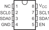
5 Pin Configuration and Functions

DGK Package
8-Pin VSSOP
Top View
PCA9515B po_cps232.gif
NC - No internal connection

Pin Functions

PIN I/O DESCRIPTION
NO. NAME
1 NC No internal connection
2 SCL0 I/O Serial clock bus 0
3 SDA0 I/O Serial data bus 0
4 GND Supply ground
5 EN I Active-high repeater enable input
6 SDA1 I/O Serial data bus 1
7 SCL1 I/O Serial clock bus 1
8 VCC Supply power