SBBS002B January   1994  – June 2015 OPT101

PRODUCTION DATA.  

  1. Features
  2. Applications
  3. Description
  4. Revision History
  5. Pin Configuration and Functions
  6. Specifications
    1. 6.1 Absolute Maximum Ratings
    2. 6.2 ESD Ratings
    3. 6.3 Recommended Operating Conditions
    4. 6.4 Thermal Information
    5. 6.5 Electrical Characteristics
    6. 6.6 Electrical Characteristics: Photodiode
    7. 6.7 Electrical Characteristics: Op Amp
    8. 6.8 Typical Characteristics
  7. Parameter Measurement Information
    1. 7.1 Light Source Positioning and Uniformity
  8. Detailed Description
    1. 8.1 Overview
    2. 8.2 Functional Block Diagram
    3. 8.3 Feature Description
      1. 8.3.1 Dark Performance
      2. 8.3.2 Feedback Network and Dynamic Response
        1. 8.3.2.1 Changing Responsivity
      3. 8.3.3 Noise Performance
      4. 8.3.4 Linearity Performance
      5. 8.3.5 Capacitive Load Drive
    4. 8.4 Device Functional Modes
  9. Application and Implementation
    1. 9.1 Application Information
    2. 9.2 Typical Applications
      1. 9.2.1 Color and Reflective Wavelength Tester
        1. 9.2.1.1 Design Requirements
        2. 9.2.1.2 Detailed Design Procedure
        3. 9.2.1.3 Application Curves
      2. 9.2.2 Three-Wire Remote Light Measurement
      3. 9.2.3 Differential Light Measurement
      4. 9.2.4 LED Output Regulation Circuit
    3. 9.3 Dos and Don'ts
  10. 10Power-Supply Recommendations
  11. 11Layout
    1. 11.1 Layout Guidelines
    2. 11.2 Layout Example
  12. 12Device and Documentation Support
    1. 12.1 Community Resources
    2. 12.2 Trademarks
    3. 12.3 Electrostatic Discharge Caution
    4. 12.4 Moisture Sensitivity and Soldering
    5. 12.5 Glossary
  13. 13Mechanical, Packaging, and Orderable Information

封装选项

机械数据 (封装 | 引脚)
散热焊盘机械数据 (封装 | 引脚)
订购信息

11 Layout

11.1 Layout Guidelines

Make all power connections with short, low impedance connections.

Depending on the application, the design might benefit from having the OPT101 mounted to the opposite side of the board as the other electrical components. Keeping the optical sensor side free from extra components allows for easier mounting of any required optical-mechanical structures around the OPT101.

11.2 Layout Example

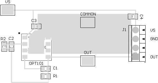
The following example shows an external feedback network (R2 and C2) that bypasses the internal feedback network, similar to Figure 19. This example also shows an external feedback network (R1, C1) in series with the internal feedback network, similar to Figure 18. To use only the internal feedback network, load R1 or C1 with a short circuit. This example allows for three different configurations with the same layout. Do not load R1, C1, R2, and C2 simultaneously.
OPT101 layout_example_sbbs002.gifFigure 30. Layout Example