ZHCSMN5 February 2021 OPA859-Q1
PRODUCTION DATA
- 1 特性
- 2 应用
- 3 说明
- 4 Revision History
- 5 Pin Configuration and Functions
- 6 Specifications
- 7 Parameter Measurement Information
- 8 Detailed Description
- 9 Application and Implementation
- 10Power Supply Recommendations
- 11Layout
- 12Device and Documentation Support
- 13Mechanical, Packaging, and Orderable Information
8.3.4 Slew Rate and Output Stage
In addition to wide bandwidth, the OPA859-Q1 features a high slew rate of 2750 V/µs. The slew rate is a critical parameter in high-speed pulse applications with narrow sub-10-ns pulses, such as optical time-domain reflectometry (OTDR) and LIDAR. The high slew rate of the OPA859-Q1 implies that the device accurately reproduces a 2-V, sub-ns pulse edge, as seen in Figure 6-20. The wide bandwidth and slew rate of the OPA859-Q1 make it an excellent amplifier for high-speed signal-chain front ends.
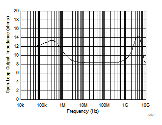
Figure 8-7 shows the open-loop output impedance of the OPA859-Q1 as a function of frequency. To achieve high slew rates and low output impedance across frequency, the output swing of the OPA859-Q1 is limited to approximately 3 V. The OPA859-Q1 is typically used in conjunction with high-speed pipeline ADCs and flash ADCs that have limited input ranges. Therefore, the OPA859-Q1 output swing range coupled with the class-leading voltage noise specification for a CMOS amplifier maximizes the overall dynamic range of the signal chain.
 Figure 8-7 Open-Loop Output Impedance
(ZOL) vs Frequency