SBOS376I November 2006 – July 2016 OPA827
PRODUCTION DATA.
- 1 Features
- 2 Applications
- 3 Description
- 4 Revision History
- 5 Pin Configuration and Functions
- 6 Specifications
- 7 Detailed Description
- 8 Application and Implementation
- 9 Power Supply Recommendations
- 10Layout
- 11Device and Documentation Support
- 12Mechanical, Packaging, and Orderable Information
8 Application and Implementation
NOTE
Information in the following applications sections is not part of the TI component specification, and TI does not warrant its accuracy or completeness. TI’s customers are responsible for determining suitability of components for their purposes. Customers should validate and test their design implementation to confirm system functionality.
8.1 Application Information
The OPA827 is a unity-gain stable, operational amplifier with very low noise, input bias current, and input offset voltage. Applications with noisy or high-impedance power supplies require decoupling capacitors placed close to the device pins. In most cases, 0.1-µF capacitors are adequate. Designers can easily take advantage of the low-noise characteristics of JFET amplifiers while also interfacing to modern, single-supply, precision data converters.
8.2 Typical Application
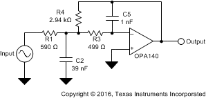
 Figure 48. 25-kHz Low-Pass Filter
8.2.1 Design Requirements
Low-pass filters are commonly employed in signal processing applications to reduce noise and prevent aliasing. The OPA827 is ideally suited to construct high-speed, high-precision active filters. Figure 48 shows a second-order, low-pass filter commonly encountered in signal processing applications.
Use the following parameters for this design example:
- Gain = 5 V/V (inverting gain)
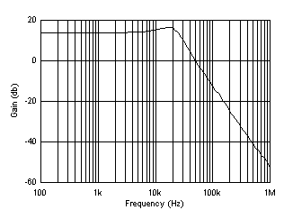
- Low-pass cutoff frequency = 25 kHz
- Second-order Chebyshev filter response with 3-dB gain peaking in the pass band
8.2.2 Detailed Design Procedure
The infinite-gain multiple-feedback circuit for a low-pass network function is shown in. Use Equation 3 to calculate the voltage transfer function.

This circuit produces a signal inversion. For this circuit, the gain at DC and the low-pass cutoff frequency are calculated by Equation 4.

Software tools are readily available to simplify filter design. WEBENCH® Filter Designer is a simple, powerful, and easy-to-use active filter design program. WEBENCH® Filter Designer lets you create optimized filter designs using a selection of TI operational amplifiers and passive components from TI's vendor partners.
Available as a web based tool from the WEBENCH Design Center, WEBENCH Filter Designer allows you to design, optimize, and simulate complete multistage active filter solutions within minutes.
8.2.3 Application Curve
 Figure 49. OPA827 Second-Order, 25-kHz, Chebyshev, Low-Pass Filter
8.3 System Examples
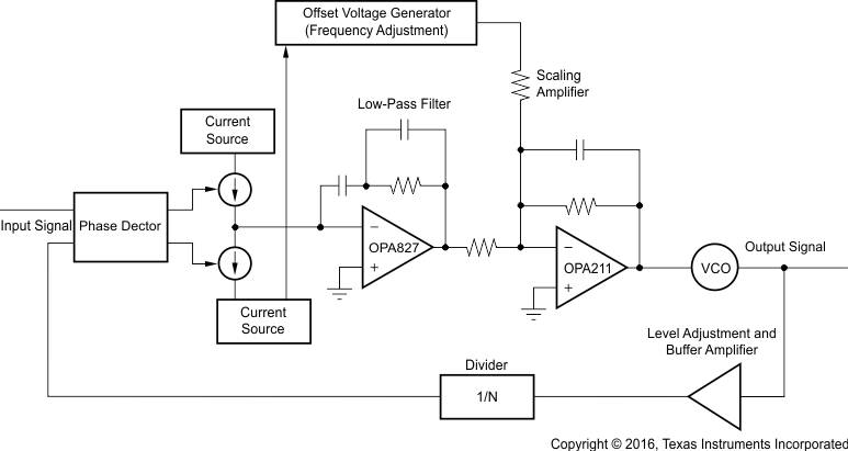
The OPA827 is well-suited for phase-lock loop (PLL) applications because of the low voltage offset, low noise, and wide gain bandwidth. Figure 50 illustrates an example of the OPA827 in this application. The first amplifier (OPA827) provides the loop low-pass, active filter function, while the second amplifier (OPA211) serves as a scaling amplifier. This second stage amplifies the DC error voltage to the appropriate level before it is applied to the voltage-controlled oscillator (VCO).
Operational amplifiers used in PLL applications are often required to have low voltage offset. As with other DC levels generated in the loop, a voltage offset applied to the VCO is interpreted as a phase error. An operational amplifier with inherently low voltage offset helps reduce this source of error. Also, any noise produced by the operational amplifiers modulates the voltage applied to the VCO and limits the spectral purity of the oscillator output. The VCO generates noise-related, random phase variations of its own, but this characteristic becomes worse when the input voltage source noise is included. This noise appears as random sideband energy that can limit system performance. The very low flicker noise (1/f) and current noise (In) of the OPA827 help to minimize the operational amplifier contribution to the phase noise.
 Figure 50. PLL Application
8.3.1 OPA827 Used as an I/V Converter
The OPA827 series of operation amplifiers have low current noise and offset voltage that make these devices a great choice for an I/V converter. DAC8811 is a single-channel, current output, 16-bit digital-to-analog converter (DAC). The IOUT terminal of the DAC is held at a virtual GND potential by the use of the OPA827 as an external I/V converter op amp. The R-2R ladder is connected to an external reference input (VREF) that determines the DAC full-scale current. The external reference voltage can vary in a range of –15 V to 15 V, thus providing bipolar IOUT current operation. By using the OPA827 as an external I/V converter in conjunction with the internal DAC8811 RFB resistor, output voltage ranges of –VREF to +VREF can be generated.
When using an external I/V converter and the DAC8811 RFB resistor, the DAC output voltage is given by Equation 5.

NOTE
CODE is the digital input into the DAC.
The DAC output impedance as seen looking into the IOUT terminal changes versus code. The low offset voltage of the OPA827 minimizes the error propagated from the DAC.
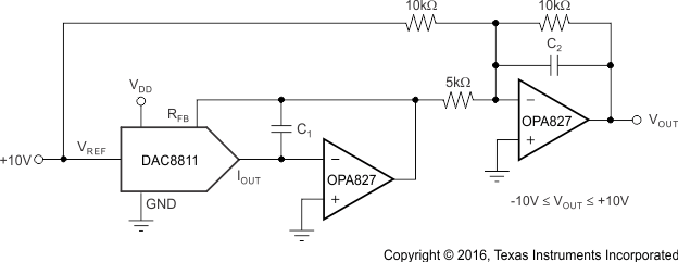
For a current-to-voltage design (see Figure 51), the DAC8811 IOUT pin and the inverting node of the OPA827 must be as short as possible and adhere to good PCB layout design. For each code change on the output of the DAC, there is a step function. If the parasitic capacitance is excessive at the inverting node, then gain peaking is possible. For circuit stability, two compensation capacitors, C1 and C2 (4 pF to 20 pF typical) can be added to the design.
Some applications require full four-quadrant multiplying capabilities or a bipolar output swing. As shown in Figure 51, the OPA827 is added as a summing amp and has a gain of 2x that widens the output span to 20 V. A four-quadrant multiplying circuit is implemented by using a 10-V offset of the reference voltage to bias the OPA827.
 Figure 51. I/V Converter