ZHCSFL2D October   2016  – June 2019 OPA2325 , OPA325 , OPA4325

PRODUCTION DATA.  

  1. 特性
  2. 应用
    1.     失调电压与输入共模电压间的关系
  3. 说明
    1.     可用作 ADC 驱动放大器的 OPAx325
  4. 修订历史记录
  5. Pin Configuration and Functions
    1.     Pin Functions: OPA325
    2.     Pin Functions: OPA2325
    3.     Pin Functions: OPA4325
  6. Specifications
    1. 6.1 Absolute Maximum Ratings
    2. 6.2 ESD Ratings
    3. 6.3 Recommended Operating Conditions
    4. 6.4 Thermal Information: OPA325
    5. 6.5 Thermal Information: OPA2325
    6. 6.6 Thermal Information: OPA4325
    7. 6.7 Electrical Characteristics: VS = 2.2 V to 5.5 V or ±1.1 V to ±2.75 V
    8. 6.8 Typical Characteristics
  7. Detailed Description
    1. 7.1 Overview
    2. 7.2 Functional Block Diagram
    3. 7.3 Feature Description
      1. 7.3.1 Zero-Crossover Input Stage
      2. 7.3.2 Low Input Offset Voltage
      3. 7.3.3 Input and ESD Protection
    4. 7.4 Device Functional Modes
  8. Application and Implementation
    1. 8.1 Application Information
      1. 8.1.1 Operating Characteristics
      2. 8.1.2 Basic Amplifier Configurations
      3. 8.1.3 Driving an Analog-to-Digital Converter
    2. 8.2 Typical Application
      1. 8.2.1 Design Requirements
      2. 8.2.2 Detailed Design Procedure
      3. 8.2.3 Application Curves
  9. Power Supply Recommendations
  10. 10Layout
    1. 10.1 Layout Guidelines
    2. 10.2 Layout Example
  11. 11器件和文档支持
    1. 11.1 文档支持
      1. 11.1.1 相关文档
    2. 11.2 相关链接
    3. 11.3 接收文档更新通知
    4. 11.4 社区资源
    5. 11.5 商标
    6. 11.6 静电放电警告
    7. 11.7 Glossary
  12. 12机械、封装和可订购信息

封装选项

机械数据 (封装 | 引脚)
散热焊盘机械数据 (封装 | 引脚)
订购信息

Low Input Offset Voltage

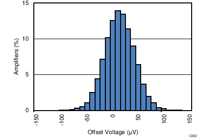
The OPAx325 are manufactured using TI's e-trim technology. Each amplifier is trimmed in production, thereby minimizing errors associated with input offset voltage. The e-trim technology is a TI proprietary method of trimming internal device parameters during either wafer probing or final testing. This process allows the OPAx325 to have an excellent offset specification of 150 µV (maximum). Figure 42 shows the offset voltage distribution for the OPAx325.
OPA325 OPA2325 OPA4325 C002_SBOS637.pngFigure 42. Offset Voltage Distribution