ZHCSD05 November 2014 OPA4277-EP
PRODUCTION DATA.
6 Specifications
6.1 Absolute Maximum Ratings
over operating free-air temperature (unless otherwise noted) (1)| MIN | MAX | UNIT | ||
|---|---|---|---|---|
| Supply voltage | 36 | V | ||
| Input voltage | (V–) – 0.7 | (V+) + 0.7 | V | |
| Output short circuit | Continuous | |||
| Operating temperature | –55 | 125 | °C | |
| Junction temperature | 150 | °C | ||
| Lead temperature (soldering, 10 s) | 300 | °C | ||
(1) Stresses beyond those listed under Absolute Maximum Ratings may cause permanent damage to the device. These are stress ratings only, which do not imply functional operation of the device at these or any other conditions beyond those indicated under Recommended Operating Conditions. Exposure to absolute-maximum-rated conditions for extended periods may affect device reliability.
6.2 Handling Ratings
| MIN | MAX | UNIT | |||
|---|---|---|---|---|---|
| Tstg | Storage temperature range | –55 | 125 | °C | |
| V(ESD) | Electrostatic discharge | Human body model (HBM), per ANSI/ESDA/JEDEC JS-001, all pins(1) | –2000 | 2000 | V |
| Machine model (MM) | –100 | 100 | |||
(1) JEDEC document JEP155 states that 500-V HBM allows safe manufacturing with a standard ESD control process.
6.3 Recommended Operating Conditions
over operating free-air temperature range (unless otherwise noted)| MIN | MAX | UNIT | ||
|---|---|---|---|---|
| Dual supply voltage | ±5 | ±15 | V | |
| TJ | Operating junction temperature | –55 | 125 | °C |
6.4 Thermal Information
| THERMAL METRIC(1) | OPA4277-EP | UNIT | |
|---|---|---|---|
| D (14 PINS) | |||
| RθJA | Junction-to-ambient thermal resistance | 66.3 | °C/W |
| RθJC(top) | Junction-to-case (top) thermal resistance | 19.3 | |
| RθJB | Junction-to-board thermal resistance | 26.8 | |
| ψJT | Junction-to-top characterization parameter | 2.1 | |
| ψJB | Junction-to-board characterization parameter | 26.2 | |
| RθJC(bot) | Junction-to-case (bottom) thermal resistance | N/A | |
(1) For more information about traditional and new thermal metrics, see the IC Package Thermal Metrics application report, SPRA953.
6.5 Electrical Characteristics
At TJ = 25°C, and RL = 2 kΩ, VS = ±5 to ±15 V (unless otherwise noted)| PARAMETER | TEST CONDITIONS | MIN | TYP | MAX | UNIT | |
|---|---|---|---|---|---|---|
| OFFSET VOLTAGE | ||||||
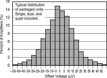
| VOS | Input offset voltage | ±20 | ±65 | µV | ||
| Input offset voltage over temperature | TJ = –55°C to 125°C | ±140 | ||||
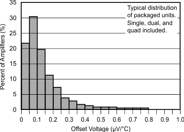
| dVOS/dT | Input offset voltage drift | ±0.15 | µV/°C | |||
| PSRR | Input offset voltage | vs time | 0.2 | µV/mo | ||
| vs power supply, VS = ±2 to ±18 V | ±0.3 | ±1 | µV/V | |||
| TJ = –55°C to 125°C; VS = ±2 to ±18 V |
±1 | µV/V | ||||
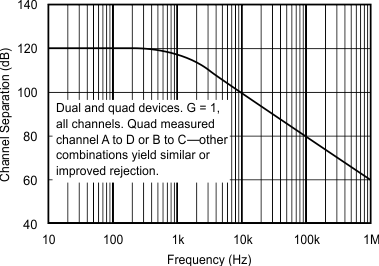
| Channel separation | dc | 0.1 | µV/V | |||
| INPUT BIAS CURRENT | ||||||
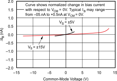
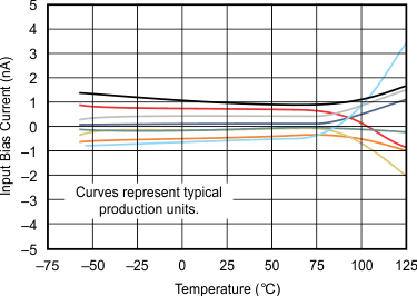
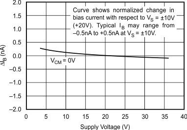
| IB | Input bias current | ±0.5 | ±2.8 | nA | ||
| TJ = –55°C to 125°C | ±7.5 | |||||
| IOS | Input offset current | ±0.5 | ±2.8 | nA | ||
| TJ = –55°C to 125°C | ±7.5 | |||||
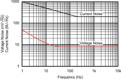
| NOISE | ||||||
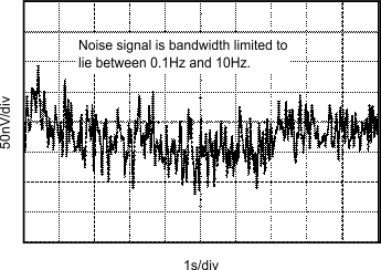
| Input voltage noise | ƒ = 0.1 to 10 Hz | 0.22 | µVpp | |||
| en | Input voltage noise density | ƒ = 10 Hz | 12 | nV/√Hz | ||
| ƒ = 100 Hz | 8 | |||||
| ƒ = 1 kHz | 8 | |||||
| ƒ = 10 kHz | 8 | |||||
| in | Current noise density | ƒ = 1 kHz | 0.2 | pA/√Hz | ||
| INPUT VOLTAGE | ||||||
| VCM | Common-mode voltage range | (V–) + 2 | (V+) – 2 | V | ||
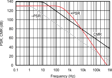
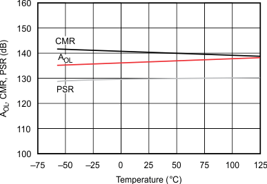
| CMRR | Common-mode rejection | VCM = (V–) + 2 V to (V+) – 2 V | 115 | 140 | dB | |
| TJ = –55°C to 125°C; VCM = (V–) + 2 V to (V+) – 2 V | 115 | |||||
| INPUT IMPEDANCE | ||||||
| Differential | 100 || 3 | MΩ || pF | ||||
| Common mode | VCM = (V–) + 2 V to (V+) – 2 V | 250 || 3 | GΩ || pF | |||
| OPEN-LOOP GAIN | ||||||
| AOL | Open-loop voltage gain | VO = (V–) + 0.5 V to (V+) – 1.2 V, RL = 10 kΩ |
140 | dB | ||
| VO = (V–) + 1.5 V to (V+) – 1.5 V, RL = 2 kΩ |
126 | 134 | ||||
| TJ = –55°C to 125°C; VO = (V–) + 1.5 V to (V+) – 1.5 V, RL = 2 kΩ | 126 | |||||
| FREQUENCY RESPONSE | ||||||
| GBW | Gain-bandwidth product | 1 | MHz | |||
| SR | Slew rate | 0.8 | V/µs | |||
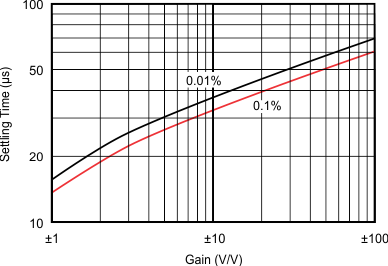
| Setting time | 0.1%, VS = ±15 V, G = 1, 10-V step | 14 | µs | |||
| 0.01%, VS = ±15 V, G = 1, 10-V step | 16 | |||||
| THD + N | Total harmonic distortion + noise | 1 kHz, G = 1, VO = 3.5 Vrms | 0.002% | |||
| OUTPUT | ||||||
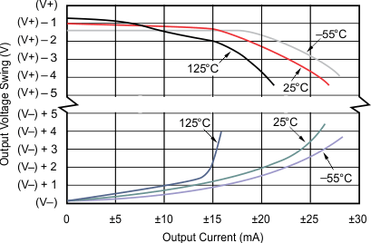
| VO | Voltage output | TJ = –55°C to 125°C; RL = 10 kΩ | (V–) + 0.5 | (V+) – 1.2 | V | |
| TJ = –55°C to 125°C; RL = 2 kΩ | (V–) + 1.5 | (V+) – 1.5 | ||||
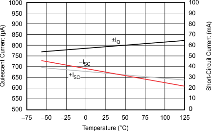
| ISC | Short-circuit current | ±35 | mA | |||
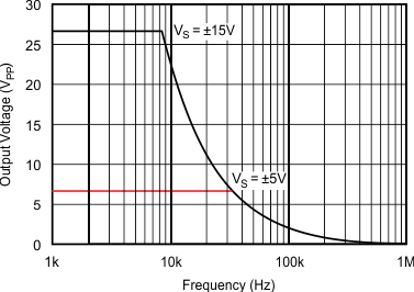
| CLOAD | Capacitive load drive | See Typical Characteristics | ||||
| POWER SUPPLY | ||||||
| VS | Specified voltage | ±5 | ±15 | V | ||
| Operating voltage | ±2 | ±18 | V | |||
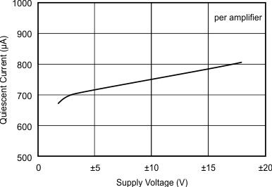
| IQ | Quiescent current (per amplifier) | IO = 0 | ±790 | ±825 | µA | |
| TJ = –55°C to 125°C; IO = 0 | ±900 | |||||
6.6 Typical Characteristics
At TJ = 25°C, VS = ±15 V, and RL = 2 kΩ, unless otherwise noted.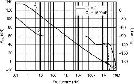
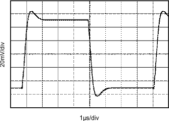
| 10-V step | CL = 1500 pF |
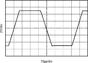
| G = 1 | CL = 1500 pF | VS = 15 V |
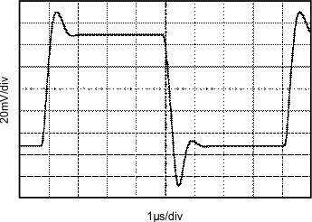
| G = 1 | CL = 1500 pF | VS = 15 V |
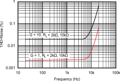
| VOUT = 3.5 Vrms |
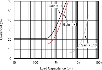
| G = 1 | CL = 0 pF | VS = 15 V |