SBOS406G June 2007 – December 2015 OPA2376 , OPA376 , OPA4376
PRODUCTION DATA.
- 1 Features
- 2 Applications
- 3 Description
- 4 Revision History
- 5 Pin Configuration and Functions
- 6 Specifications
- 7 Detailed Description
- 8 Application and Implementation
- 9 Power Supply Recommendations
- 10Layout
- 11Device and Documentation Support
- 12Mechanical, Packaging, and Orderable Information
封装选项
机械数据 (封装 | 引脚)
散热焊盘机械数据 (封装 | 引脚)
订购信息
12 Mechanical, Packaging, and Orderable Information
The following pages include mechanical, packaging, and orderable information. This information is the most current data available for the designated devices. This data is subject to change without notice and revision of this document. For browser-based versions of this data sheet, refer to the left-hand navigation.
The OPAx376 are specified for operation from 2.2 V to 5.5 V (±1.1 V to ±2.75 V); many specifications apply from –40°C to +125°C. Parameters that can exhibit significant variance with regard to operating voltage or temperature are presented in the Typical Characteristics.
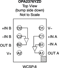
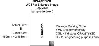
The OPA2376YZD is a lead (Pb)-free, die-level, die-size ball grid array (DSBGA) package. Unlike devices that are in plastic packages, these devices have no molding compound, lead frame, wire bonds, or leads. Using standard surface-mount assembly procedures, the DSBGA can be mounted to a printed circuit board (PCB) without additional underfill. Figure 33 and Figure 34 detail the pinout and package marking. See Application Note SBVA017, NanoStar™ and NanoFree™ 300 μm Solder Bump WCSP, for more detailed information on package characteristics and PCB design.
 Figure 33. Pin Description
 Figure 34. Top-View Package Marking