ZHCSCS6B September   2014  – December 2018 OPA2320-Q1 , OPA320-Q1

PRODUCTION DATA.  

  1. 特性
  2. 应用
  3. 说明
    1.     零交叉失真:低偏移电压
  4. 修订历史记录
  5. Pin Configuration and Functions
    1.     Pin Functions
  6. Specifications
    1. 6.1 Absolute Maximum Ratings
    2. 6.2 ESD Ratings
    3. 6.3 Recommended Operating Conditions
    4. 6.4 Thermal Information
    5. 6.5 Electrical Characteristics:
    6. 6.6 Typical Characteristics
  7. Detailed Description
    1. 7.1 Overview
    2. 7.2 Functional Block Diagram
    3. 7.3 Feature Description
      1. 7.3.1 Input and ESD Protection
      2. 7.3.2 Feedback Capacitor Improves Response
      3. 7.3.3 EMI Susceptibility And Input Filtering
      4. 7.3.4 Output Impedance
      5. 7.3.5 Capacitive Load and Stability
      6. 7.3.6 Overload Recovery Time
    4. 7.4 Device Functional Modes
      1. 7.4.1 Rail-to-Rail Input
      2. 7.4.2 Phase Reversal
  8. Application and Implementation
    1. 8.1 Application Information
    2. 8.2 Typical Applications
      1. 8.2.1 Transimpedance Amplifier
        1. 8.2.1.1 Design Requirements
        2. 8.2.1.2 Detailed Design Procedure
          1. 8.2.1.2.1 Optimizing The Transimpedance Circuit
        3. 8.2.1.3 Application Curves
      2. 8.2.2 High-Impedance Sensor Interface
      3. 8.2.3 Driving ADCs
      4. 8.2.4 Active Filter
  9. Power Supply Recommendations
  10. 10Layout
    1. 10.1 Layout Guidelines
    2. 10.2 Layout Example
  11. 11器件和文档支持
    1. 11.1 器件支持
      1. 11.1.1 开发支持
    2. 11.2 相关链接
    3. 11.3 接收文档更新通知
    4. 11.4 社区资源
    5. 11.5 商标
    6. 11.6 静电放电警告
    7. 11.7 术语表
  12. 12机械、封装和可订购信息

封装选项

机械数据 (封装 | 引脚)
散热焊盘机械数据 (封装 | 引脚)
订购信息

Transimpedance Amplifier

Wide gain bandwidth, low input bias current, low input voltage, and current noise make the OPAx320-Q1 an excellent wideband photodiode transimpedance amplifier. Low-voltage noise is important because photodiode capacitance causes the effective noise gain of the circuit to increase at high frequency.

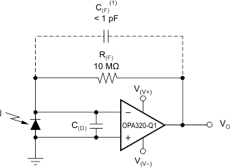
The key elements to a transimpedance design, as shown in Figure 36, are the expected diode capacitance (C(D)), which should include the parasitic input common-mode and differential-mode input capacitance (4 pF + 5 pF); the desired transimpedance gain (R(FB)); and the gain-bandwidth (GBW) for the OPAx320-Q1 (20 MHz). With these three variables set, the feedback capacitor value (C(FB)) can be set to control the frequency response. C(FB) includes the stray capacitance of R(FB), which is 0.2 pF for a typical surface-mount resistor.
OPA320-Q1 OPA2320-Q1 ai_trans_amp_dual_slos884.gif

NOINDENT:

C(FB) is optional to prevent gain peaking. C(FB) includes the stray capacitance of R(FB).
Figure 36. Dual-Supply Transimpedance Amplifier