ZHCSJ01B January   2019  – August 2019 OPA1671

PRODUCTION DATA.  

  1. 特性
  2. 应用
  3. 说明
    1.     Device Images
      1.      驻极体麦克风前置放大器
      2.      OPA1671 电压噪声密度
  4. 修订历史记录
  5. Pin Configuration and Functions
    1.     Pin Functions
  6. Specifications
    1. 6.1 Absolute Maximum Ratings
    2. 6.2 ESD Ratings
    3. 6.3 Recommended Operating Conditions
    4. 6.4 Thermal Information
    5. 6.5 Electrical Characteristics
    6. 6.6 Typical Characteristics
  7. Detailed Description
    1. 7.1 Overview
    2. 7.2 Functional Block Diagram
    3. 7.3 Feature Description
      1. 7.3.1 Operating Voltage
      2. 7.3.2 Input Bias Current
      3. 7.3.3 Common-Mode Voltage Range
      4. 7.3.4 EMI Susceptibility and Input Filtering
    4. 7.4 Device Functional Modes
  8. Application and Implementation
    1. 8.1 Application Information
      1. 8.1.1 Capacitive Loads
      2. 8.1.2 Noise Performance
      3. 8.1.3 Basic Noise Calculations
    2. 8.2 Typical Application
      1. 8.2.1 Design Requirements
      2. 8.2.2 Detailed Design Procedure
      3. 8.2.3 Application Curves
  9. Power Supply Recommendations
  10. 10Layout
    1. 10.1 Layout Guidelines
    2. 10.2 Layout Example
  11. 11器件和文档支持
    1. 11.1 器件支持
      1. 11.1.1 开发支持
        1. 11.1.1.1 TINA-TI(免费软件下载)
    2. 11.2 文档支持
      1. 11.2.1 相关文档
    3. 11.3 接收文档更新通知
    4. 11.4 社区资源
    5. 11.5 商标
    6. 11.6 静电放电警告
    7. 11.7 Glossary
  12. 12机械、封装和可订购信息

封装选项

机械数据 (封装 | 引脚)
散热焊盘机械数据 (封装 | 引脚)
订购信息

Basic Noise Calculations

Low-noise circuit design requires careful analysis of all noise sources. External noise sources can dominate in many cases; consider the effect of source resistance on overall op amp noise performance. Total noise of the circuit is the root-sum-square combination of all noise components.

The resistive portion of the source impedance produces thermal noise proportional to the square root of the resistance. This function is plotted in Figure 31. The source impedance is typically fixed; consequently, select the op amp and the feedback resistors to minimize the respective contributions to the total noise.

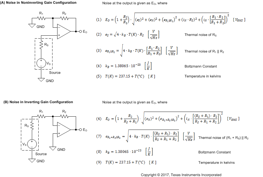
Figure 33 shows noninverting (A) and inverting (B) op amp circuit configurations with gain. In circuit configurations with gain, the feedback network resistors contribute noise. In general, the current noise of the op amp reacts with the feedback resistors to create additional noise components.

The selected feedback resistor values make these noise sources negligible. Low impedance feedback resistors load the output of the amplifier. The equations for total noise are shown for both configurations.
OPA1671 S008_SBOS427.gif
eN is the voltage noise of the amplifier. For the OPA1671 series of operational amplifiers, eN = 4.0 nV/√Hz at 10 kHz.
iN is the current noise of the amplifier. For the OPA1671 series of operational amplifiers, iN = 4.5 fA/√Hz at 1 kHz.
For additional resources on noise calculations, see TI's Precision Labs Series.
Figure 33. Noise Calculation in Gain Configurations