ZHCSEV2C January   2016  – September 2016 MUX508 , MUX509

PRODUCTION DATA.  

  1. 特性
  2. 应用
  3. 说明
  4. 修订历史记录
  5. Device Comparison Table
  6. Pin Configuration and Functions
  7. Specifications
    1. 7.1 Absolute Maximum Ratings
    2. 7.2 ESD Ratings
    3. 7.3 Recommended Operating Conditions
    4. 7.4 Thermal Information
    5. 7.5 Electrical Characteristics: Dual Supply
    6. 7.6 Electrical Characteristics: Single Supply
    7. 7.7 Typical Characteristics
  8. Parameter Measurement Information
    1. 8.1  Truth Tables
    2. 8.2  On-Resistance
    3. 8.3  Off-Leakage Current
    4. 8.4  On-Leakage Current
    5. 8.5  Transition Time
    6. 8.6  Break-Before-Make Delay
    7. 8.7  Turn-On and Turn-Off Time
    8. 8.8  Charge Injection
    9. 8.9  Off Isolation
    10. 8.10 Channel-to-Channel Crosstalk
    11. 8.11 Bandwidth
    12. 8.12 THD + Noise
  9. Detailed Description
    1. 9.1 Overview
    2. 9.2 Functional Block Diagram
    3. 9.3 Feature Description
      1. 9.3.1 Ultralow Leakage Current
      2. 9.3.2 Ultralow Charge Injection
      3. 9.3.3 Bidirectional Operation
      4. 9.3.4 Rail-to-Rail Operation
    4. 9.4 Device Functional Modes
  10. 10Applications and Implementation
    1. 10.1 Application Information
    2. 10.2 Typical Application
      1. 10.2.1 Design Requirements
      2. 10.2.2 Detailed Design Procedure
      3. 10.2.3 Application Curve
  11. 11Power-Supply Recommendations
  12. 12Layout
    1. 12.1 Layout Guidelines
    2. 12.2 Layout Example
  13. 13器件和文档支持
    1. 13.1 文档支持
      1. 13.1.1 相关文档 
    2. 13.2 相关链接
    3. 13.3 接收文档更新通知
    4. 13.4 社区资源
    5. 13.5 商标
    6. 13.6 静电放电警告
    7. 13.7 Glossary
  14. 14机械、封装和可订购信息

封装选项

机械数据 (封装 | 引脚)
散热焊盘机械数据 (封装 | 引脚)
订购信息

Layout

Layout Guidelines

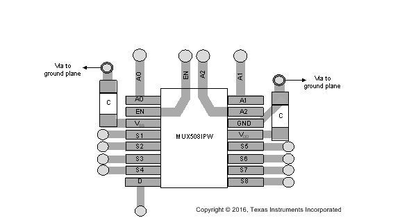
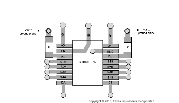
Figure 45 shows an example of a PCB layout with the MUX508IPW, and Figure 46 shows an example of a PCB layout with MUX509IPW. The guidelines provided in this section are also applicable to the SOIC MUX508ID and MUX509ID package variants as well.

Some key considerations are:

  1. Decouple the VDD and VSS pins with a 0.1-µF capacitor, placed as close to the pin as possible. Make sure that the capacitor voltage rating is sufficient for the VDD and VSS supplies.
  2. Keep the input lines as small as possible. For the MUX509 differential signals, make sure the A inputs and B inputs are as symmetric as possible.
  3. Use a solid ground plane to help distribute heat and reduce electromagnetic interference (EMI) noise pickup.
  4. Do not run sensitive analog traces in parallel with digital traces. Avoid crossing digital and analog traces if possible and only make perpendicular crossings when necessary.

Layout Example

MUX508 MUX509 layout_mux508_sbas758.gif Figure 45. MUX508IPW Layout Example
MUX508 MUX509 layout_mux509_sbas758.gif Figure 46. MUX509IPW Layout Example