ZHCS707D December 2011 – September 2018 MSP430F6720 , MSP430F6721 , MSP430F6723 , MSP430F6724 , MSP430F6725 , MSP430F6726 , MSP430F6730 , MSP430F6731 , MSP430F6733 , MSP430F6734 , MSP430F6735 , MSP430F6736
PRODUCTION DATA.
- 1器件概述
- 2修订历史记录
- 3Device Comparison
- 4Terminal Configuration and Functions
-
5Specifications
- 5.1 Absolute Maximum Ratings
- 5.2 ESD Ratings
- 5.3 Recommended Operating Conditions
- 5.4 Active Mode Supply Current Into VCC Excluding External Current
- 5.5 Low-Power Mode Supply Currents (Into VCC) Excluding External Current
- 5.6 Low-Power Mode With LCD Supply Currents (Into VCC) Excluding External Current
- 5.7 Thermal Resistance Characteristics
- 5.8
Digital I/O Ports
- Table 5-1 Schmitt-Trigger Inputs – General-Purpose I/O
- Table 5-2 Inputs – Ports P1 and P2
- Table 5-3 Leakage Current – General-Purpose I/O
- Table 5-4 Outputs – General-Purpose I/O (Full Drive Strength)
- Table 5-5 Typical Characteristics – General-Purpose I/O (Full Drive Strength)
- Table 5-6 Outputs – General-Purpose I/O (Reduced Drive Strength)
- 5.8.1 Typical Characteristics – General-Purpose I/O (Reduced Drive Strength)
- Table 5-7 Output Frequency – General-Purpose I/O
- 5.9 Clock Specifications
- 5.10 Power-Management Module (PMM)
- 5.11
Auxiliary Supplies
- Table 5-19 Auxiliary Supplies, Recommended Operating Conditions
- Table 5-20 Auxiliary Supplies, AUXVCC3 (Backup Subsystem) Currents
- Table 5-21 Auxiliary Supplies, Auxiliary Supply Monitor
- Table 5-22 Auxiliary Supplies, Switch ON-Resistance
- Table 5-23 Auxiliary Supplies, Switching Time
- Table 5-24 Auxiliary Supplies, Switch Leakage
- Table 5-25 Auxiliary Supplies, Auxiliary Supplies to ADC10_A
- Table 5-26 Auxiliary Supplies, Charge Limiting Resistor
- 5.12 Timer_A
- 5.13 eUSCI
- 5.14 LCD Controller
- 5.15
SD24_B
- Table 5-36 SD24_B Power Supply and Recommended Operating Conditions
- Table 5-37 SD24_B Analog Input
- Table 5-38 SD24_B Supply Currents
- Table 5-39 SD24_B Performance
- Table 5-40 SD24_B AC Performance
- Table 5-41 SD24_B AC Performance
- Table 5-42 SD24_B AC Performance
- Table 5-43 SD24_B External Reference Input
- 5.16 ADC10_A
- 5.17 REF
- 5.18 Flash Memory
- 5.19 Emulation and Debug
-
6Detailed Description
- 6.1 CPU
- 6.2 Instruction Set
- 6.3 Operating Modes
- 6.4 Interrupt Vector Addresses
- 6.5 Memory Organization
- 6.6 Bootloader (BSL)
- 6.7 JTAG Operation
- 6.8 Flash Memory
- 6.9 RAM
- 6.10 Backup RAM
- 6.11
Peripherals
- 6.11.1 Oscillator and System Clock
- 6.11.2 Power Management Module (PMM)
- 6.11.3 Auxiliary Supply System
- 6.11.4 Backup Subsystem
- 6.11.5 Digital I/O
- 6.11.6 Port Mapping Controller
- 6.11.7 System Module (SYS)
- 6.11.8 Watchdog Timer (WDT_A)
- 6.11.9 DMA Controller
- 6.11.10 CRC16
- 6.11.11 Hardware Multiplier
- 6.11.12 Enhanced Universal Serial Communication Interface (eUSCI)
- 6.11.13 ADC10_A
- 6.11.14 SD24_B
- 6.11.15 TA0
- 6.11.16 TA1
- 6.11.17 TA2
- 6.11.18 TA3
- 6.11.19 SD24_B Triggers
- 6.11.20 ADC10_A Triggers
- 6.11.21 Real-Time Clock (RTC_C)
- 6.11.22 Reference (REF) Module Voltage Reference
- 6.11.23 LCD_C
- 6.11.24 Embedded Emulation Module (EEM) (S Version)
- 6.11.25 Peripheral File Map
- 6.12
Input/Output Diagrams
- 6.12.1 Port P1 (P1.0 and P1.1) Input/Output With Schmitt Trigger (MSP430F67xxIPZ and MSP430F67xxIPN)
- 6.12.2 Port P1 (P1.2) Input/Output With Schmitt Trigger (MSP430F67xxIPZ and MSP430F67xxIPN)
- 6.12.3 Port P1 (P1.3 to P1.5) Input/Output With Schmitt Trigger (MSP430F67xxIPZ and MSP430F67xxIPN)
- 6.12.4 Port P1 (P1.6 and P1.7) (MSP430F67xxIPZ and MSP430F67xxIPN), Port P2 (P2.0 and P2.1) (MSP430F67xxIPZ Only) Input/Output With Schmitt Trigger
- 6.12.5 Port P2 (P2.2 to P2.7) Input/Output With Schmitt Trigger (MSP430F67xxIPZ Only)
- 6.12.6 Port P3 (P3.0 to P3.3) Input/Output With Schmitt Trigger (MSP430F67xxIPZ Only)
- 6.12.7 Port P3 (P3.4 to P3.7) Input/Output With Schmitt Trigger (MSP430F67xxIPZ Only)
- 6.12.8 Port P4 (P4.0 to P4.7), Port P5 (P5.0 to P5.7), Port P6 (P6.0 to P6.7), Port P7 (P7.0 to P7.7), Port P8 (P8.0 to P8.3) Input/Output With Schmitt Trigger (MSP430F67xxIPZ Only)
- 6.12.9 Port P8 (P8.4 to P8.7) Input/Output With Schmitt Trigger (MSP430F67xxIPZ Only)
- 6.12.10 Port P9 (P9.0) Input/Output With Schmitt Trigger (MSP430F67xxIPZ Only)
- 6.12.11 Port P9 (P9.1 to P9.3) Input/Output With Schmitt Trigger (MSP430F67xxIPZ Only)
- 6.12.12 Port P2 (P2.0 and P2.1) Input/Output With Schmitt Trigger (MSP430F67xxIPN Only)
- 6.12.13 Port P2 (P2.2 to P2.7) Input/Output With Schmitt Trigger (MSP430F67xxIPN Only)
- 6.12.14 Port P3 (P3.0 to P3.7) Input/Output With Schmitt Trigger (MSP430F67xxIPN Only)
- 6.12.15 Port P4 (P4.0 to P4.7), Port P5 (P5.0 to P5.7), Port P6 (P6.0 to P6.7) Input/Output With Schmitt Trigger (MSP430F67xxIPN Only)
- 6.12.16 Port PJ (PJ.0) JTAG Pin TDO, Input/Output With Schmitt Trigger or Output
- 6.12.17 Port PJ (PJ.1 to PJ.3) JTAG Pins TMS, TCK, TDI/TCLK, Input/Output With Schmitt Trigger or Output
- 6.13 Device Descriptors (TLV)
- 7器件和文档支持
- 8机械、封装和可订购信息
4.1 Pin Diagrams
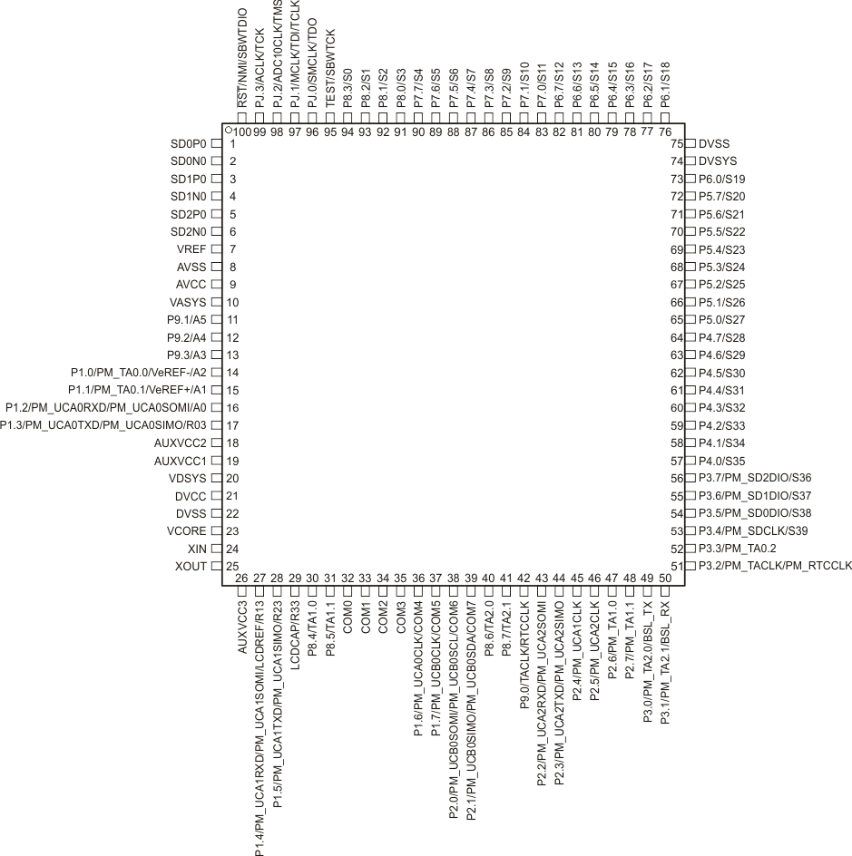
Figure 4-1 shows the pinout for the 100-pin PZ package. See Table 4-1 for differences between the MSP430F673x and MSP430F672x devices in this package.

NOTE:
The secondary digital functions on Ports P1, P2, and P3 are fully mappable. This pinout shows the default mapping. See Table 6-9 for details.NOTE:
The pins VDSYS and DVSYS must be connected externally on board for proper device operation.CAUTION:
The LCDCAP/R33 pin must be connected to DVSS if not used.Table 4-1 Pinout Differences Between MSP430F673xIPZ and MSP430F672xIPZ(1)
| PIN NUMBER | PIN NAME | |
|---|---|---|
| MSP430F673xIPZ | MSP430F672xIPZ | |
| 1 | SD0P0 | SD0P0 |
| 2 | SD0N0 | SD0N0 |
| 3 | SD1P0 | SD1P0 |
| 4 | SD1N0 | SD1N0 |
| 5 | SD2P0 | NC |
| 6 | SD2N0 | NC |
| 7 | VREF | VREF |
| 53 | P3.4/PM_SDCLK/S39 | P3.4/PM_SDCLK/S39 |
| 54 | P3.5/PM_SD0DIO/S38 | P3.5/PM_SD0DIO/S38 |
| 55 | P3.6/PM_SD1DIO/S37 | P3.6/PM_SD1DIO/S37 |
| 56 | P3.7/PM_SD2DIO/S36 | P3.7/PM_NONE/S36 |
(1) Signal names that differ between devices are indicated by italic typeface.
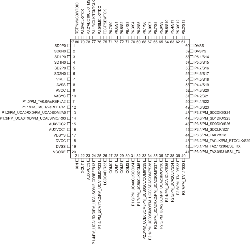
Figure 4-2 shows the pinout for the 80-pin PN package. See Table 4-2 for differences between the MSP430F673x and MSP430F672x devices in this package.

NOTE:
The secondary digital functions on Ports P1, P2, and P3 are fully mappable. This pinout shows the default mapping. See Table 6-9 for details.NOTE:
The pins VDSYS and DVSYS must be connected externally on board for proper device operation.CAUTION:
The LCDCAP/R33 pin must be connected to DVSS if not used.Table 4-2 Pinout Differences Between MSP430F673xIPN and MSP430F672xIPN(1)
| PIN NUMBER | PIN NAME | |
|---|---|---|
| MSP430F673xIPN | MSP430F672xIPN | |
| 1 | SD0P0 | SD0P0 |
| 2 | SD0N0 | SD0N0 |
| 3 | SD1P0 | SD1P0 |
| 4 | SD1N0 | SD1N0 |
| 5 | SD2P0 | NC |
| 6 | SD2N0 | NC |
| 7 | VREF | VREF |
| 45 | P3.4/PM_SDCLK/S27 | P3.4/PM_SDCLK/S27 |
| 46 | P3.5/PM_SD0DIO/S26 | P3.5/PM_SD0DIO/S26 |
| 47 | P3.6/PM_SD1DIO/S25 | P3.6/PM_SD1DIO/S25 |
| 48 | P3.7/PM_SD2DIO/S24 | P3.7/PM_NONE/S24 |