SNOSAG7D August 2005 – August 2016 LPV511
PRODUCTION DATA.
7 Detailed Description
7.1 Overview
The LPV511 is a micropower operational amplifier that operates from a voltage supply range as wide as 2.7 V to 12 V with ensured specifications at 3 V, 5 V, and 12 V. The LPV511 exhibits an excellent speed-to-power ratio, drawing only 880 nA of supply current with a bandwidth of 27 kHz.
7.2 Functional Block Diagram

7.3 Feature Description
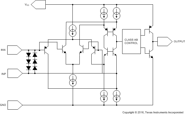
The LPV511 has a rail-to-rail input which provides more flexibility for the system designer. As can be seen from Functional Block Diagram, rail-to-rail input is achieved by using in parallel, one PNP differential pair and one NPN differential pair. When the common mode input voltage (VCM) is near V+, the NPN pair is on and the PNP pair is off. When VCM is near V−, the NPN pair is off and the PNP pair is on. When VCM is between V+ and V−, internal logic decides how much current each differential pair will get. This special logic ensures stable and low distortion amplifier operation within the entire common mode voltage range.
7.4 Device Functional Modes
7.4.1 Input Stage
Because both input stages have their own offset voltage (VOS) characteristic, the offset voltage of the LPV511 becomes a function of VCM. VOS has a crossover point at 1 V below V+. See the VOS vs VCM curve in Typical Characteristics. Caution must be taken in situations where the input signal amplitude is comparable to the VOS value and/or the design requires high accuracy. In these situations, it is necessary for the input signal to avoid the crossover point.
The input bias current, IB will change in value and polarity as the input crosses the transition region. In addition, parameters such as PSRR and CMRR which involve the input offset voltage will also be affected by changes in VCM across the differential pair transition region.
Differential input voltage is the difference in voltage between the noninverting (+) input and the inverting input (−) of the op amp. Due to the three series diodes across the two inputs, the absolute maximum differential input voltage is ±2.1 V. This may not be a problem to most conventional op amp designs; however, designers must avoid using the LPV511 as a comparator.
7.4.2 Output Stage
The LPV511 output voltage swing 100 mV from rails at 3-V supply, which provides the maximum possible dynamic range at the output. This is particularly important when operating on low supply voltages.
The LPV511 maximum output voltage swing defines the maximum swing possible under a particular output load. The LPV511 output swings 110 mV from the rail at 5-V supply with an output load of 100 kΩ.
7.4.3 Driving Capacitive Load
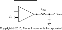
The LPV511 is internally compensated for stable unity gain operation, with a 27-kHz typical gain bandwidth. However, the unity gain follower is the most sensitive configuration to capacitive load. Direct capacitive loading reduces the phase margin of the op amp. When the output is required to drive a large capacitive load, greater than 100 pF, a small series resistor at the output of the amplifier improves the phase margin (see Figure 27).
In Figure 27, the isolation resistor RISO and the load capacitor CL form a pole to increase stability by adding more phase margin to the overall system. The desired performance depends on the value of RISO. The bigger the RISO resistor value, the more stable VOUT will be. But the DC accuracy is degraded when the RISO gets bigger. If there were a load resistor in Figure 27, the output voltage would be divided by RISO and the load resistor.
 Figure 27. Resistive Isolation of Capacitive Load