ZHCSJ52A December 2019 – August 2021 LP875701-Q1
PRODUCTION DATA
- 1 特性
- 2 应用
- 3 说明
- 4 Revision History
- 5 Pin Configuration and Functions
- 6 Specifications
-
7 Detailed Description
- 7.1 Overview
- 7.2 Functional Block Diagram
- 7.3
Feature Descriptions
- 7.3.1 Multi-Phase DC/DC Converters
- 7.3.2 Sync Clock Functionality
- 7.3.3 Power-Up
- 7.3.4 Regulator Control
- 7.3.5 Enable and Disable Sequences
- 7.3.6 Device Reset Scenarios
- 7.3.7 Diagnosis and Protection Features
- 7.3.8 GPIO Signal Operation
- 7.3.9 Digital Signal Filtering
- 7.4 Device Functional Modes
- 7.5 Programming
- 7.6
Register Maps
- 7.6.1
Register Descriptions
- 53
- 7.6.1.1 DEV_REV
- 7.6.1.2 OTP_REV
- 7.6.1.3 BUCK0_CTRL1
- 7.6.1.4 BUCK0_DELAY
- 7.6.1.5 GPIO2_DELAY
- 7.6.1.6 GPIO3_DELAY
- 7.6.1.7 RESET
- 7.6.1.8 CONFIG
- 7.6.1.9 INT_TOP1
- 7.6.1.10 INT_TOP2
- 7.6.1.11 INT_BUCK_0_1
- 7.6.1.12 INT_BUCK_2_3
- 7.6.1.13 TOP_STAT
- 7.6.1.14 BUCK_0_1_STAT
- 7.6.1.15 BUCK_2_3_STAT
- 7.6.1.16 TOP_MASK1
- 7.6.1.17 TOP_MASK2
- 7.6.1.18 BUCK_0_1_MASK
- 7.6.1.19 BUCK_2_3_MASK
- 7.6.1.20 SEL_I_LOAD
- 7.6.1.21 I_LOAD_2
- 7.6.1.22 I_LOAD_1
- 7.6.1.23 PGOOD_CTRL1
- 7.6.1.24 PGOOD_CTRL2
- 7.6.1.25 PGOOD_FLT
- 7.6.1.26 PLL_CTRL
- 7.6.1.27 PIN_FUNCTION
- 7.6.1.28 GPIO_CONFIG
- 7.6.1.29 GPIO_IN
- 7.6.1.30 GPIO_OUT
- 7.6.1
Register Descriptions
- 8 Application and Implementation
- 9 Power Supply Recommendations
- 10Layout
- 11Device and Documentation Support
- 12Mechanical, Packaging, and Orderable Information
7.3.4.1 Enabling and Disabling Regulators
One or more regulators can be enabled when the device is in STANDBY or ACTIVE state. There are two ways for enable and disable the regulators:
- Using EN_BUCK0 bit in BUCK0_CTRL1 register (EN_PIN_CTRL0 register bit is 0h)
- Using EN1, EN2, EN3 control pins (EN_BUCK0 bit is 1h AND EN_PIN_CTRL0 register bit is 1 in BUCK0_CTRL1 register)
If the EN1, EN2, EN3 control pins are used for enable and disable then the control pin is selected with BUCK0_EN_PIN_SELECT[1:0] bits (in BUCK0_CTRL1 register). The delay from the control signal rising edge to enabling of the regulator is set by BUCK0_STARTUP_DELAY[3:0] bits and the delay from control signal falling edge to disabling of the regulator is set by BUCK0_SHUTDOWN_DELAY[3:0] bits in BUCK0_DELAY register. The delays are valid only for EN1, EN2, EN3 signal control. The control with EN_BUCK0 bit is immediate without the delays.
The control of the regulator (with 0-ms delays) is shown in Table 7-3.
The control of the regulator cannot be changed from one ENx pin to a different ENx pin because the control is ENx signal edge sensitive. The control from ENx pin to register bit and back to the original ENx pin can be done during operation.
| CONTROL METHOD | EN_BUCK0 | EN_PIN_CTRL0 | BUCK0_EN_PIN_SELECT[1:0] | EN1 PIN | EN2 PIN | EN3 PIN | BUCKx OUTPUT VOLTAGE | |
|---|---|---|---|---|---|---|---|---|
| Enable and disable control with EN_BUCK0 bit | 0h | Don't Care | Don't Care | Don't Care | Don't Care | Don't Care | Disabled | |
| 1h | 0h | Don't Care | Don't Care | Don't Care | Don't Care | 1.0 Volt | ||
| Enable and disable control with EN1 pin | 1h | 1h | 0h | Low | Don't Care | Don't Care | Disabled | |
| 1h | 1h | 0h | High | Don't Care | Don't Care | 1.0 Volt | ||
| Enable and disable control with EN2 pin | 1h | 1h | 1h | Don't Care | Low | Don't Care | Disabled | |
| 1h | 1h | 1h | Don't Care | High | Don't Care | 1.0 Volt | ||
| Enable and disable control with EN3 pin | 1h | 1h | 2h | Don't Care | Don't Care | Low | Disabled | |
| 1h | 1h | 2h | Don't Care | Don't Care | High | 1.0 Volt |
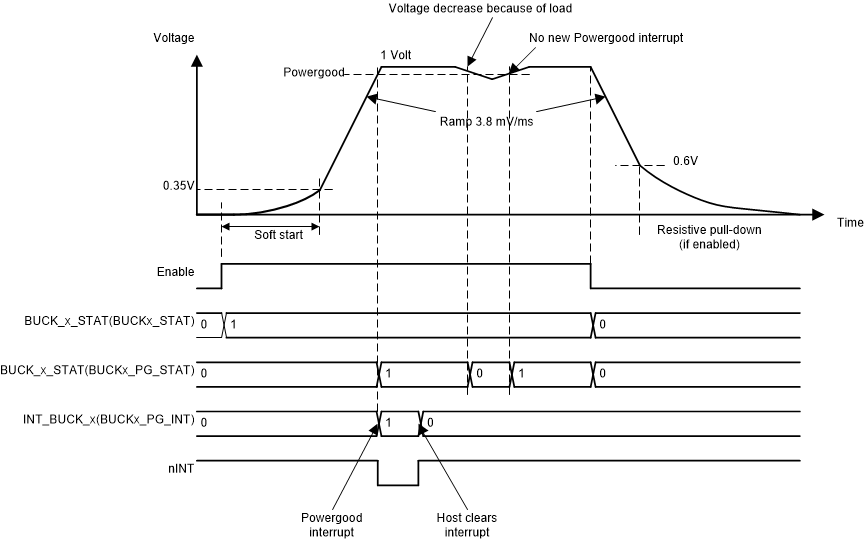
The regulator is enabled by the ENx pin or by I2C writing as shown in Figure 7-5. The soft-start circuit limits the in-rush current during start-up. When the output voltage rises to 0.35-V level, the output voltage becomes slew-rate controlled . If there is a short circuit at the output and the output voltage does not increase above 0.35-V level in 1 ms, the regulator is disabled, and interrupt is set. When the output voltage reaches the Power-Good threshold level the BUCKx_PG_INT interrupt flag (in INT_BUCK_x register) is set. The Power-Good interrupt flag can be masked using BUCKx_PG_MASK bit (in BUCKx_MASK register).
The ENx input pins have integrated pulldown resistors. The pulldown resistors are enabled by default, and the host can disable those with ENx_PD bits (in CONFIG register).
 Figure 7-5 Regulator Enable and Disable