ZHCSDA9 February 2015 LP8728D-Q1
PRODUCTION DATA.
7 Detailed Description
7.1 Overview
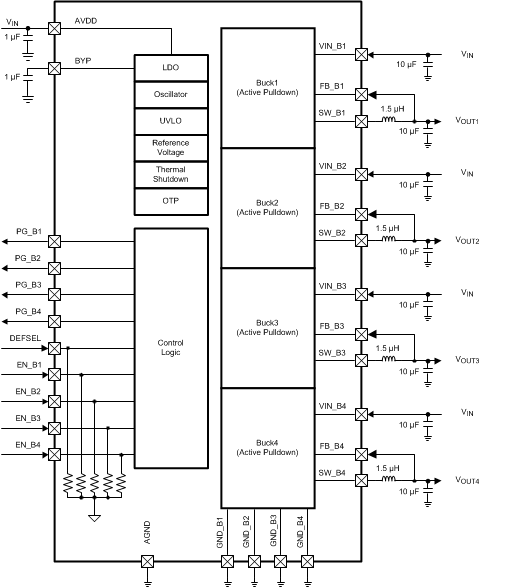
The LP8728D-Q1 has four integrated high-efficiency buck converters. Each buck converter has individual enable input and power good output pins. When the first enable pin is pulled high there is a 420-µs start-up delay when the device wakes up from the shutdown mode and all internal reference blocks are started up. Once reference blocks have settled, the corresponding buck converter turns on. Buck cores utilize the soft-start feature to limit the inrush current during start-up. Once a buck output reaches 96% (typical) of the desired output voltage, the power-good pin is pulled high (see Figure 9). When at least one buck core is active, the remaining buck converters will start up without any start-up delay.
If the output voltage drops below 93% (typical) of desired voltage due to, for example, an overload condition, the corresponding power-good pin is pulled low. The power-good signal is always held low for at least 50 ms. When the enable pin is pulled low, the corresponding buck converter's power good signals are set low, and the buck converter is instantly shut down. An output capacitor is then discharged through an internal 70-Ω (typical) pulldown resistor. The pulldown resistor is connected between buck feedback pin and ground and is only active when the enable pin is set low. When all enable signals are pulled low, the LP8728D-Q1 enters a low current shutdown mode.
7.2 Functional Block Diagram
7.3 Feature Description
7.3.1 Buck Information
The buck converters are operated in a forced PWM mode. Even with light load a minimum switching pulse is generated with every switching cycle. Each buck converter's high-side switch turn-on time is phase shifted to minimize the input current ripple (see Figure 20).
7.3.1.1 Features
The following features are supported for all converters:
- Synchronous rectification
- Current mode feedback loop with PI compensator
- Forced PWM operation
- Soft start
- Power-good output
- Overvoltage comparator
In addition to the aforementioned features, Buck3 output voltage can be selected with the DEFSEL pin. If the DEFSEL pin is pulled low, VOUT3 is set to 1.8 V. If DEFSEL is pulled high, VOUT3 is set to 2.65 V.
 Figure 9. Buck Converter Start-up And Shutdown
7.3.2 Thermal Shutdown (TSD)
Thermal shutdown function shuts down all buck regulators if the device's junction temperature TJ rises above 150°C (typ.). All power-good signals are pulled low 5 ms before the buck regulators are shut down. Once TJ falls below 130°C (typical), the LP8728 will automatically start up the buck regulators. There is a 2-second safety delay included in the restart function. Buck regulators are not restarted until 2 seconds have elapsed after TJ falls below 130°C (typical). To minimize the inrush current during restarting, regulators are started in a Buck1 → Buck2 → Buck3 → Buck4 sequence. A 500-µs delay is included between each buck start-up.
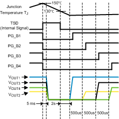 Figure 10. TSD Timing Diagram
7.3.3 Undervoltage Lockout (UVLO)
If input voltage drops below 2.7 V (typ.) the PG_Bx pins are pulled low and the buck converters are shut down. (Figure 11). The PG_Bx pins are always held low for at least 50 ms. The buck converters are restarted once the input voltage rises above UVLO level.
If a UVLO condition has lasted less than 50 ms, the PG_Bx pins are released high once 50 ms has elapsed and corresponding output voltage has settled. If an overvoltage condition has lasted more than 50 ms, the PG_Bx pins are released high once corresponding output voltage has settled.
Regulators are always restarted in a Buck1 → Buck2 → Buck3 → Buck4 sequence. A 500-µs delay is included between each buck start-up.
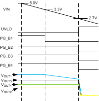 Figure 11. UVLO Operation
7.3.4 Overvoltage Protection (OVP)
Overvoltage protection protects the device in case of an overvoltage condition. If input voltage exceeds 5.7 V (typical), all PG_Bx pins are pulled low. the PG_Bx pins are always held low for at least 50 ms. Once the PG_Bx pins are pulled low, the system has 5 ms time to power down. After an overvoltage condition has lasted for 5 ms, all buck converters are shut down. The buck converters are restarted once input voltage falls below 5.62 V (typical). The buck converters are started in a Buck1 → Buck2 → Buck3 → Buck4 sequence. A 500-µs delay is included between each buck start-up.
If an overvoltage condition lasted more than 5 ms, but less than 50 ms, the PG_Bx pins are released high once 50 ms has elapsed and the corresponding output voltage has settled (Figure 12).
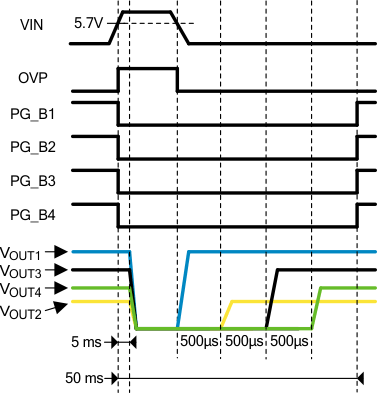 Figure 12. OVP Duration Less Than 50 ms
If an overvoltage condition has lasted more than 50 ms, the power-good signals are released high once the corresponding output voltage has settled. Regulators are started in a buck1 → buck2 → buck3 → buck4 sequence. A 500-µs delay is included between each buck start-up (Figure 13). If an overvoltage condition has lasted less than 5 ms, the buck converters are not shut down. Even in this case the PG_Bx pins are held low for 50 ms.
NOTE
Since the regulators are allowed to operate for 5 ms during overvoltage condition it is the system designer’s responsibility to verify that input voltage doesn’t exceed limits stated in Absolute Maximum Ratings. Exceeding these limits may cause permanent damage to the device.
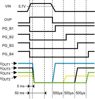 Figure 13. OVP Duration More Than 50 ms
7.4 Device Functional Modes
7.4.1 Shutdown Mode
When all EN_Bx inputs are low, the device is in a Shutdown mode. This is a low-power mode when all buck-regulators and all internal blocks are disabled.
7.4.2 Active Mode
When the first enable pin is pulled high there is a 420-µs start-up delay when the device wakes up from the Shutdown; mode and all internal reference blocks are started up. Once the reference blocks have settled, the corresponding buck converter turns on. Buck cores utilize the soft-start feature to limit the inrush current during start-up. Once a buck output reaches 96% (typical) of the desired output voltage, the power-good pin is pulled high. When at least one buck converter is active device is in a Active mode. When device is in Active mode, the remaining buck converters will start up without any start-up delay when EN_Bx pin is pulled high. When EN_Bx pin is set low the corresponding buck converter will shut down. When all EN_Bx pins are set low the device shuts down all internal reference blocks and enters Shutdown mode.
If output voltage of a buck regulator falls below 93% (typical) of desired voltage due to, for example, an overload condition, the corresponding power good pin is pulled low. Once the output voltage rises back above 96% (typical) of desired voltage power good pin is set back high. Power good signal is held low for at least 50 ms.
If OVP, or TSD fault occurs during normal operation, all power good pins are pulled low. Once fault condition has lasted for 5 ms all buck converters are shut down. In case of UVLO fault buck regulators are instantly shut down. Once fault condition has ended buck converters are restarted in a Buck1 → Buck2 → Buck3 → Buck4 power-up sequence. A 500-µs delay is included between each buck start-up. In case of TSD fault there is a 2-second safety delay before power-up sequence.
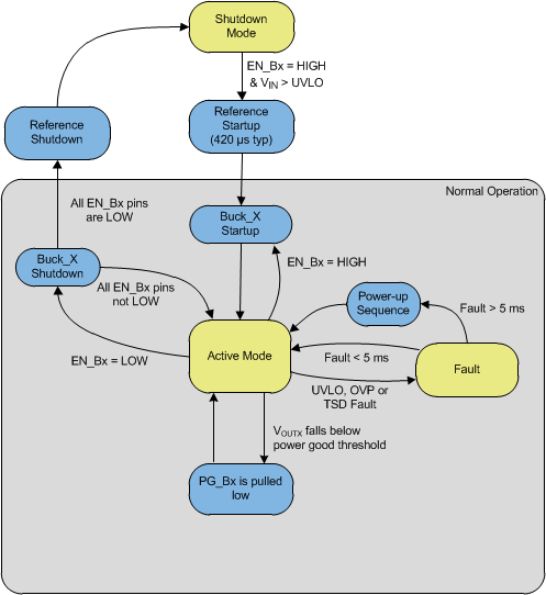 Figure 14. Device Functional Modes