SNVS857 February 2014 LP8555
PRODUCTION DATA.
- 1 Features
- 2 Applications
- 3 Description
- 4 Simplified Schematic
- 5 Revision History
- 6 Terminal Configuration and Functions
- 7 Specifications
-
8 Detailed Description
- 8.1 Overview
- 8.2 Functional Block Diagram
- 8.3
Features Description
- 8.3.1 Boost Converter Overview
- 8.3.2 Brightness Control
- 8.3.3 LED Brightness Slopes, Normal and Advanced
- 8.3.4
Start-up and Shutdown Sequences
- 8.3.4.1 Start-up With PWM Input Brightness Control Mode (BRTMODE = 00b)
- 8.3.4.2 Shutdown With PWM Input Brightness Control Mode (BRTMODE = 00b)
- 8.3.4.3 Start-up With I2C Brightness Control Mode (BRTMODE = 01b)
- 8.3.4.4 Shutdown With I2C Brightness Control Mode (BRTMODE = 01b)
- 8.3.4.5 Start-up with I2C + PWM Input Brightness Control Mode (BRTMODE = 10 or 11b)
- 8.3.4.6 Shutdown with I2C + PWM Input Brightness Control Mode (BRTMODE = 10 or 11b)
- 8.3.5 LED String Count Auto Detection
- 8.3.6 Fault Detection
- 8.3.7 I2C-Compatible Serial Bus Interface
- 8.4 Device Functional Modes
- 8.5
Register Maps
- 8.5.1 COMMAND
- 8.5.2 STATUS/MASK
- 8.5.3 BRTLO
- 8.5.4 BTHI
- 8.5.5 CONFIG
- 8.5.6 CURRENT
- 8.5.7 PGEN
- 8.5.8 BOOST
- 8.5.9 LEDEN
- 8.5.10 STEP
- 8.5.11 Brightness Transitions, Typical Times
- 8.5.12 VOLTAGE_0
- 8.5.13 LEDEN1
- 8.5.14 VOLTAGE1
- 8.5.15 OPTION
- 8.5.16 EXTRA
- 8.5.17 ID
- 8.5.18 REVISION
- 8.5.19 CONF0
- 8.5.20 CONF1
- 8.5.21 VHR0
- 8.5.22 VHR1
- 8.5.23 JUMP
-
9 Application and Implementation
- 9.1 Application Information
- 9.2 Typical Applications
- 10Power Supply Recommendations
- 11Layout
- 12 Device and Documentation Support
- 13Mechanical, Packaging, and Orderable Information
7 Specifications
7.1 Absolute Maximum Ratings(1)
Over operating free-air temperature range (unless otherwise noted)| MIN | MAX | UNIT | ||
|---|---|---|---|---|
| VDD | Voltage on VDD | –0.3 | 22 | V |
| VLDO | Voltage on VLDO | –0.3 | 6 | |
| V(PWM/INT, EN/VDDIO/ FSET/SDA, ISET/SCL) | Voltage on logic terminals | |||
| V(SW_A, SW_B, LEDxy, FB_x) | Voltage on analog terminals | –0.3 | 31 | |
| PD | Continuous Power Dissipation (3) | Internally limited | ||
| TA | Operating ambient temperature range (5) | –40 | 85 | °C |
| TJ | Maximum operating junction temperature (5) | –40 | 125 | |
| Tsoldering | Note (4) |
(1) Stresses beyond those listed under absolute maximum ratings may cause permanent damage to the device. These are stress ratings only, and functional operation of the device at these or any other conditions beyond those indicated under recommended operating conditions is not implied. Exposure to absolute–maximum–rated conditions for extended periods may affect device reliability.
7.2 Handling Ratings
| MIN | MAX | UNIT | ||
|---|---|---|---|---|
| TSTORAGE | Storage temp range | –65 | 150 | °C |
| VHBM | Human body model (HBM) voltage(1) | 2000 | V | |
| VCDM | Charged device model (CDM) (2) | 250 | ||
(1) Level listed above is the passing level per ANSI/ESDA/JEDEC JS-001. JEDEC document JEP155 states that 500-V HBM allows safe manufacturing with a standard ESD control process. Terminals listed as 2 kV may actually have higher performance.
(2) Level listed above is the passing level per EIA-JEDEC JESD22-C101. JEDEC document JEP157 states that 250-V CDM allows safe manufacturing with a standard ESD control process. Terminals listed as 250 V may actually have higher performance
7.3 Recommended Operating Conditions(1)(2)
Over operating free-air temperature range (unless otherwise noted)| MIN | MAX | UNIT | ||
|---|---|---|---|---|
| VDD – Voltage on VDD | 2.7 | 20 | V | |
| VLDO – Voltage on VLDO | 2.7 | 5.5 | ||
| V (EN/VDDIO) – Supply voltage for digital I/O | 1.7 | 5.5 | ||
| V (PWM/INT, FSET/SDA, ISET/SCL) – Voltage on logic terminals | 0 | 5.5 | ||
| V (SW_A, SW_B, LEDxy, FB_x) | 0 | 28 | ||
7.4 Thermal Information
Over operating free-air temperature range (unless otherwise noted)| THERMAL METRIC(1) | DSBGA (36 TERMINALS) |
UNIT | |
|---|---|---|---|
| θJA | Junction-to-ambient thermal resistance (θJA) (6) | 76.2 | °C/W |
| θJC | Junction-to-case (top) thermal resistance | 0.3 | °C/W |
| θJB | Junction-to-board thermal resistance | 16.3 | °C/W |
| ΨJT | Junction-to-top characterization parameter | 1.8 | °C/W |
| ΨJB | Junction-to-board characterization parameter | 16.3 | °C/W |
(1) For more information about traditional and new thermal metrics, see the IC Package Thermal Metrics application report, SPRA953.
7.5 Electrical Characteristics(2)(7)
Limits apply over the full ambient temperature range –40°C ≤ TA ≤ 85°C. Unless otherwise specified: VDD = 3.6 V, EN/VDDIO = 1.8 V, L1 = L2 = 6.8 µH, CIN_A = CIN_B = 10 µF, COUT_A = COUT_B = 10 µF, CVLDO = 10 µF, CVDD = 1 µF.(8)| PARAMETER | TEST CONDITIONS | MIN | TYP | MAX | UNIT | |
|---|---|---|---|---|---|---|
| IIN | Shutdown supply current | EN = L and PWM/INT = L | 1 | µA | ||
| Standby supply current | EN = H and PWM/INT = L, ON bit = 0 | 19 | 30 | |||
| Normal mode supply current | EN = H, ON bit = 1, no current going through LED outputs | 4.2 | mA | |||
| fOSC | Internal oscillator frequency accuracy | -7% | 7% | |||
| TTSD | Thermal shutdown threshold | 150 | °C | |||
| TTSD_hyst | Thermal shutdown hysteresis | 13 | ||||
| tSTART-UP | Start-up time(9) | 5 | 7 | ms | ||
| BOOST CONVERTER (Applies for both boost converters) | ||||||
| VBST_MIN | Minimum output voltage | 7 | V | |||
| VBST_MAX | Maximum output voltage | VMAX = 00 VMAX = 01 VMAX = 10 VMAX = 11 |
18 22 25 28 |
V | ||
| IMAX | SW FET current limit | 2.7 | 3.1 | 3.5 | A | |
| RNMOS | NMOS switch-ON resistance | ISW = 0.5 A | 0.16 | Ω | ||
| ILOAD | Continuous load current | VBATT = 3 V, VOUT = 26.6 V. Typical application. | 180 | mA | ||
| ƒSW | Switching frequency | BFREQ = 0 BFREQ = 1 |
500 1000 |
kHz | ||
| ƒSW_ACCURACY | Boost oscillator accuracy | –7% | 7% | |||
| VOVP_THR | Overvoltage protection voltage threshold | VBST_MAX +1.6 V |
V | |||
| VOUT/VIN | Conversion ratio | No load, BFREQ = 1 | 1.3 | 10 | ||
| ΔVSW/toff-on | SW node voltage slew rate during OFF-to-ON transition | Load current 120 mA. Boost slew rate set to fastest (SRON = 00b). | 12.5 | V/ns | ||
| ΔVSW/ton-off | SW node voltage slew rate during ON-to-OFF transition | 19.5 | ||||
| ƒMOD | Modulation frequency (percentage of the SW frequency) | FMOD_DIV = 00 FMOD_DIV = 01 FMOD_DIV = 10 FMOD_DIV = 11 |
0.47% 0.27% 0.17% 0.12% |
|||
| CURRENT SINKS | ||||||
| ILEAKAGE | Leakage current | Outputs LEDA1...LEDB6, VLEDxx = 28 V | 1 | µA | ||
| IMAX | Maximum sink current LEDA1...B6 | 50 | mA | |||
| IOUT | Output current accuracy(10) | Output current set to 23 mA. Current scale set to 23 mA. PWM = 100% |
–4% | 4% | ||
| IMATCH | Matching (10) | 1% | 5% | |||
| ƒLED_PWM | LED switching frequency | PFREQ = 000b PFREQ = 111b |
4.9 39.1 |
kHz | ||
| VSAT | Saturation voltage (11) | Output current set to 23 mA | 200 | 260 | mV | |
| Output current set to 30 mA | 250 | 340 | ||||
| PWM INTERFACE CHARACTERISTICS | ||||||
| ƒPWM | PWM input frequency | 75 | 50000 | Hz | ||
| tMIN_ON | Minimum pulse ON time | 100 | ns | |||
| tMIN_OFF | Minimum pulse OFF time | 100 | ||||
| tstart-up | Turn-on delay from standby to backlight on | PWM input active, ON bit written high | 7 | ms | ||
| tSTBY | Turn-off delay | PWM input low time before entering standby mode (if PWMSB = 1) | 52 | ms | ||
| PWMRES | PWM input resolution | ƒIN < 2.4 kHz ƒIN < 4.8 kHz ƒIN < 9.6 kHz ƒIN < 19.5 kHz ƒIN < 25 kHz ƒIN < 50 kHz |
12 12 11 10 9 8 |
bits | ||
| UNDERVOLTAGE PROTECTION | ||||||
| VUVLO | VDD UVLO threshold voltage | VDD falling | 2.5 | V | ||
| VDD rising | 2.6 | |||||
| LOGIC INTERFACE | ||||||
| Logic Input EN/VDDIO | ||||||
| VEN/VDDIO | Supply voltage range | 1.7 | 5.5 | V | ||
| II | Input current | 20 | µA | |||
| Logic Input PWM/INT, FSET/SDA, ISET/SCL | ||||||
| VIL | Input low level | 0.3 x EN/VDDIO | V | |||
| VIH | Input high level | 0.7 x EN/VDDIO | V | |||
| II | Input current, VIO = 1.7 V to 5.5 V | -1.0 | 1.0 | µA | ||
| Logic Output FSET/SDA, PWM/INT | ||||||
| VOL | Output low level | IPULL-UP = 3 mA | 0.3 | 0.4 | V | |
(1) Stresses beyond those listed under Absolute Maximum Ratings may cause permanent damage to the device. These are stress ratings only, and functional operation of the device a these or any other conditions beyond those indicated under Recommended Operating Conditions is not implied. Exposure to absolute-maximum-rated conditions for extended periods may affect device reliability.
(2) All voltages are with respect to the potential at the GND terminals.
(3) Internal thermal shutdown circuitry protects the device from permanent damage. Thermal shutdown engages at TJ = 150°C (typ.) and disengages at TJ = 137°C (typ.).
(4) For detailed soldering specifications and information, please refer to Application Note AN1112.
(5) In applications where high power dissipation and/or poor package thermal resistance is present, the maximum ambient temperature may have to be degraded. Maximum ambient temperature (TA-MAX) is dependent on the maximum operating junction temperature (TJ-MAX-OP = 125ºC), the maximum power dissipation of the device in the application (PD-MAX), and the junction-to ambient thermal resistance of the part/package in the application (θJA), as given by the following equation: TA-MAX = TJ-MAX-OP – (θJA × PD-MAX).
(6) Junction-to-ambient thermal resistance is highly application and board-layout dependent. In applications where high maximum power dissipation exists, special care must be paid to thermal dissipation issues in board design.
(7) Min and Max limits are specified by design, test, or statistical analysis.
(8) Low-ESR Surface-Mount Ceramic Capacitors (MLCCs) used in setting electrical characteristics
(9) Start-up time is measured from the moment the ON bit is set high to the moment when backlight is enabled.
(10) Output Current Accuracy is the difference between the actual value of the output current and programmed value of this current. Matching is the maximum difference from the average. For the constant current sinks on the part (OUTA1 to OUTB6), the following are determined: the maximum output current (MAX), the minimum output current (MIN), and the average output current of all outputs (AVG). Matching number is calculated: (MAX-MIN)/AVG. The typical specification provided is the most likely norm of the matching figure for all parts. LED current sinks were characterized with 1 V headroom voltage. Note that some manufacturers have different definitions in use.
(11) Saturation voltage is defined as the voltage when the LED current has dropped 10% from the value measured at 1 V.
7.6 I2C Serial Bus Timing Parameters (FSET/SDA, ISET/SCL)
| MIN | TYP | MAX | UNIT | ||
|---|---|---|---|---|---|
| fSCL | Clock Frequency | 400 | kHz | ||
| 1 | Hold Time (repeated) START Condition | 0.6 | μs | ||
| 2 | Clock Low Time | 1.3 | μs | ||
| 3 | Clock High Time | 600 | ns | ||
| 4 | Setup Time for a Repeated START Condition | 600 | ns | ||
| 5 | Data Hold Time | 50 | ns | ||
| 6 | Data Setup Time | 100 | ns | ||
| 7 | Rise Time of SDA and SCL | 20+0.1xCb | 300 | ns | |
| 8 | Fall Time of SDA and SCL | 15+0.1xCb | 300 | ns | |
| 9 | Set-up Time for STOP condition | 600 | ns | ||
| 10 | Bus Free Time between a STOP and a START Condition | 1.3 | μs | ||
| Cb | Capacitive Load Parameter for Each Bus Line. Load of One Picofarad Corresponds to One Nanosecond. |
10 | 200 | ns | |
| tresponse | Delay from EN/VDDIO rising to I2C bus active | 1 | ms | ||
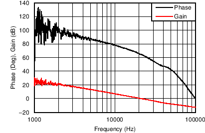
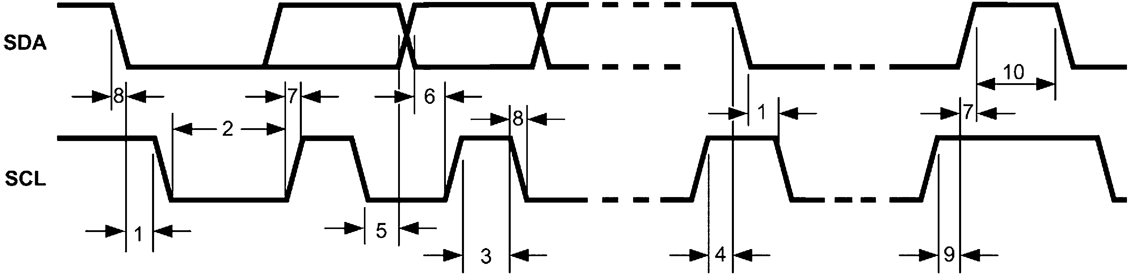 Figure 1. I2C Timing Parameters
7.7 Typical Characteristics
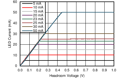
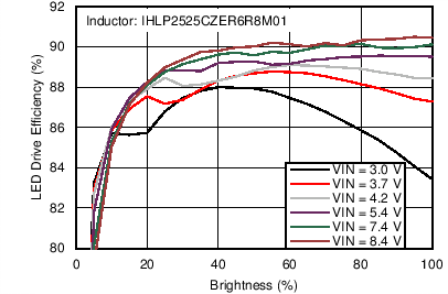
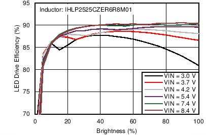
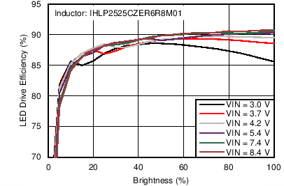
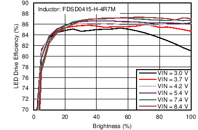
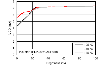
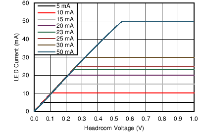
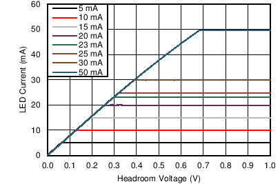
Measured at room temperature unless otherwise noted. Maximum LED current set to 23 mA per string. DC-DC Efficiency is defined as POUT/PIN, where POUT is total output power measured from boost output(s). LED Drive Efficiency is defined as PLED/PIN , where PLED is actual power consumed in LEDs.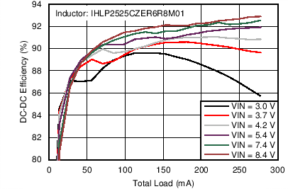
| L = 6.8 µH | 12 x 6 LEDs | +25°C |
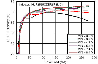
| L = 6.8 µH | 12 x 7 LEDs | +25°C |
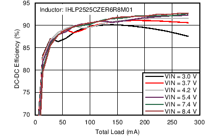
| L = 6.8 µH | 12 x 7 LEDs | -40°C |
| L = 6.8 µH | 12 x 7 LEDs | +85°C |
| L = 4.7 µH | 12 x 6 LEDs | +25°C |
| L = 4.7 µH | 12 x 7 LEDs | +25°C |
| VDD = 3.7 V | 12 x 7 LEDs |
| L = 4.7 µH | VDD = 3.7V | VBOOST = 23 V |
| IOUT = 138 mA/boost | ||
| -40°C | VDD = 3.7 V |
| L = 6.8 µH | 12 x 6 LEDs | +25°C |
| L = 6.8 µH | 12 x 7 LEDs | +25°C |
| L = 6.8 µH | 12 x 7 LEDs | -40°C |
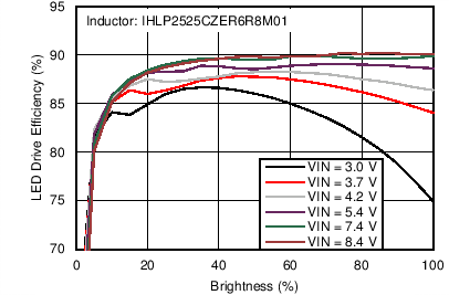
| L = 6.8 µH | 12 x 7 LEDs | +85°C |
| L = 4.7 µH | 12 x 6 LEDs | +25°C |
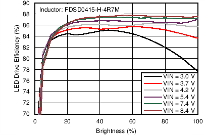
| L = 4.7 µH | 12 x 7 LEDs | +25°C |
| VDD = 3.7 V | 12 x 7 LEDs |
| +25°C | VDD = 3.7 V |
| +85°C | VDD = 3.7 V |