SNVS693E September 2011 – September 2014 LP8552
PRODUCTION DATA.
- 1 Features
- 2 Applications
- 3 Description
- 4 Revision History
- 5 Default EEPROM Values
- 6 Pin Configuration and Functions
-
7 Specifications
- 7.1 Absolute Maximum Ratings
- 7.2 Handling Ratings
- 7.3 Recommended Operating Conditions
- 7.4 Thermal Information
- 7.5 Electrical Characteristics
- 7.6 Boost Converter Electrical Characteristics
- 7.7 LED Driver Electrical Characteristics
- 7.8 PWM Interface Characteristics
- 7.9 Undervoltage Protection
- 7.10 Logic Interface Characteristics
- 7.11 I2C Serial Bus Timing Parameters (SDA, SCLK)
- 7.12 Typical Characteristics
-
8 Detailed Description
- 8.1 Overview
- 8.2 Functional Block Diagram
- 8.3
Feature Description
- 8.3.1 Clock Generation
- 8.3.2
Brightness Control Methods
- 8.3.2.1 PWM Input Duty Cycle
- 8.3.2.2 Brightness Register Control
- 8.3.2.3 PWM Direct Control
- 8.3.2.4 PWM Calculation Data Flow
- 8.3.2.5 PWM Detector
- 8.3.2.6 Brightness Control
- 8.3.2.7 Resolution Selector
- 8.3.2.8 Sloper
- 8.3.2.9 PWM & Current Control
- 8.3.2.10 Dither
- 8.3.2.11 PWM Comparator
- 8.3.2.12 Current Setting
- 8.3.2.13 PWM Frequency Setting
- 8.3.2.14 Phase Shift PWM Scheme
- 8.3.2.15 Slope And Dithering
- 8.3.2.16 Driver Headroom Control
- 8.3.3 Boost Converter
- 8.3.4 Fault Detection
- 8.4 Device Functional Modes
- 8.5 Programming
- 8.6 Register Maps
- 9 Application and Implementation
- 10Power Supply Recommendations
- 11Layout
- 12Device and Documentation Support
- 13Mechanical, Packaging, and Orderable Information
7 Specifications
7.1 Absolute Maximum Ratings(1)(2)
over operating free-air temperature range (unless otherwise noted)| MIN | MAX | UNIT | ||
|---|---|---|---|---|
| VIN | –0.3 | 24 | V | |
| VLDO | –0.3 | 6 | ||
| Voltage on logic pins (VSYNC, PWM, EN, SCLK, SDA) | –0.3 | 6 | ||
| Voltage on logic pin (FAULT) | –0.3 | VVDDIO + 0.3 | ||
| Voltage on analog pins (FILTER, VDDIO, ISET, FSET) | –0.3 | 6 | ||
| V (OUT1...OUT6, SW, FB) | –0.3 | 44 | ||
| Continuous power dissipation (3) | Internally Limited | |||
| Junction temperature (TJ-MAX) | 125 | °C | ||
| Maximum lead temperature (soldering) | See (4) | |||
(1) Stresses beyond those listed under Absolute Maximum Ratings may cause permanent damage to the device. These are stress ratings only, which do not imply functional operation of the device at these or any other conditions beyond those indicated under Recommended Operating Conditions. Exposure to absolute-maximum-rated conditions for extended periods may affect device reliability.
(2) If Military/Aerospace specified devices are required, please contact the TI Sales Office/Distributors for availability and specifications.
(3) Internal thermal shutdown circuitry protects the device from permanent damage. Thermal shutdown engages at TJ = 150°C (typ.) and disengages at TJ = 130°C (typ.).
(4) For detailed soldering specifications and information, please refer to Application Report AN-1112 DSBGA Wafer Level Chip Scale Package (SNVA009).
7.2 Handling Ratings
| MIN | MAX | UNIT | |||
|---|---|---|---|---|---|
| Tstg | Storage temperature range | –65 | 150 | °C | |
| V(ESD) | Electrostatic discharge | Human body model (HBM), per ANSI/ESDA/JEDEC JS-001, all pins(1) | -2 | 2 | kV |
| Charged device model (CDM), per JEDEC spec. JESD22-C101, all pins(2) | –200 | 200 | V | ||
| Machine model | –1 | 1 | kV | ||
(1) JEDEC document JEP155 states that 500-V HBM allows safe manufacturing with a standard ESD control process.
(2) JEDEC document JEP157 states that 250-V CDM allows safe manufacturing with a standard ESD control process.
7.3 Recommended Operating Conditions(1)(2)
over operating free-air temperature range (unless otherwise noted)| MIN | NOM | MAX | UNIT | ||
|---|---|---|---|---|---|
| VIN (Figure 27) | Input voltage | 5.5 | 22 | V | |
| VIN + VLDO (Figure 31) | 4.5 | 5.5 | |||
| VDDIO | 1.65 | 5 | |||
| V(OUT1...OUT6, SW, FB) | 0 | 40 | |||
| TJ | Junction temperature | –30 | 125 | °C | |
| TA(3) | Ambient temperature | –30 | 85 | ||
(1) Stresses beyond those listed under Absolute Maximum Ratings may cause permanent damage to the device. These are stress ratings only, which do not imply functional operation of the device at these or any other conditions beyond those indicated under Recommended Operating Conditions. Exposure to absolute-maximum-rated conditions for extended periods may affect device reliability.
(2) All voltages are with respect to the potential at the GND pins.
(3) In applications where high power dissipation and/or poor package thermal resistance is present, the maximum ambient temperature may have to be derated. Maximum ambient temperature (TA-MAX) is dependent on the maximum operating junction temperature (TJ-MAX-OP = 125°C), the maximum power dissipation of the device in the application (PD-MAX), and the junction-to ambient thermal resistance of the part/package in the application (RθJA), as given by the following equation: TA-MAX = TJ-MAX-OP – (RθJA × PD-MAX).
7.4 Thermal Information
| THERMAL METRIC(1) | DSBGA | UNIT | |
|---|---|---|---|
| 25 PINS | |||
| RθJA | Junction-to-ambient thermal resistance (2) | 40 - 73 | °C/W |
(1) For more information about traditional and new thermal metrics, see the IC Package Thermal Metrics application report, SPRA953.
(2) Junction-to-ambient thermal resistance is highly application and board-layout dependent. In applications where high maximum power dissipation exists, special care must be paid to thermal dissipation issues in board design.
7.5 Electrical Characteristics(1)(2)
Limits are for TA = 25°C (unless otherwise specified); VIN = 12 V, VDDIO = 2.8 V, CVLDO = 1 μF, L1 = 15 μH, CIN = 10 μF, COUT = 10 μF. RISET = 16 kΩ, unless otherwise specified. (3)| PARAMETER | TEST CONDITIONS | MIN | TYP | MAX | UNIT | |
|---|---|---|---|---|---|---|
| IIN | Standby supply current | Internal LDO disabled EN=L and PWM=L |
1 (4) | μA | ||
| Normal mode supply current | LDO enabled, boost enabled, no current going through LED outputs 5-MHz PLL Clock |
3 | mA | |||
| 10-MHz PLL Clock | 3.7 | |||||
| 20-MHz PLL Clock | 4.7 | |||||
| 40-MHz PLL Clock | 6.7 | |||||
| fOSC | Internal oscillator frequency accuracy | –4% –7% (4) |
4% 7%(4) |
|||
| VLDO | Internal LDO voltage | 4.5 (4) | 5 | 5.5 (4) | V | |
| ILDO | Internal LDO external loading | 5 | mA | |||
(1) All voltages are with respect to the potential at the GND pins.
(2) Minimum (MIN) and Maximum (MAX) limits are specified by design, test, or statistical analysis. Typical numbers represent the most likely norm.
(3) Low-ESR Surface-Mount Ceramic Capacitors (MLCCs) used in setting electrical characteristics.
(4) Limits apply over the full operating ambient temperature range (–30°C ≤ TA ≤ 85°C).
7.6 Boost Converter Electrical Characteristics
Limits are for TA = 25°C (unless otherwise specified); VIN = 12 V, VDDIO = 2.8 V, CVLDO = 1 μF, L1 = 15 μH, CIN = 10 μF, COUT = 10 μF. RISET = 16 kΩ, unless otherwise specified. (1)| PARAMETER | TEST CONDITIONS | MIN | TYP | MAX | UNIT | |
|---|---|---|---|---|---|---|
| RDSON | Switch ON resistance | ISW = 0.5 A | 0.12 | Ω | ||
| VMAX | Boost maximum output voltage | 40 | V | |||
| ILOAD | Maximum continuous load current | 9 V ≤ VBATT, VOUT = 35 V | 450 | mA | ||
| 6 V ≤ VBATT, VOUT = 35 V | 300 | |||||
| 3 V ≤ VBATT, VOUT = 25 V | 180 | |||||
| VOUT/VIN | Conversion ratio | fSW = 1.25 MHz | 10 | |||
| fSW | Switching frequency | BOOST_FREQ = 00 BOOST_FREQ = 01 BOOST_FREQ = 10 BOOST_FREQ = 11 |
156 312 625 1250 |
kHz | ||
| VOV | Overvoltage protection voltage | VBOOST + 1.6V | V | |||
| tPULSE | Switch pulse minimum width | no load | 50 | ns | ||
| tSTARTUP | Start-up time | Note (2) | 6 | ms | ||
| IMAX | SW pin current limit | BOOST_IMAX = 0 BOOST_IMAX = 1 |
1.4 2.5 |
A | ||
(1) Low-ESR Surface-Mount Ceramic Capacitors (MLCCs) used in setting electrical characteristics.
(2) Start-up time is measured from the moment boost is activated until the VOUT crosses 90% of its target value.
7.7 LED Driver Electrical Characteristics
Limits are for TA = 25°C (unless otherwise specified); VIN = 12 V, VDDIO = 2.8 V, CVLDO = 1 μF, L1 = 15 μH, CIN = 10 μF, COUT = 10 μF. RISET = 16 kΩ, unless otherwise specified. (1)| PARAMETER | TEST CONDITIONS | MIN | TYP | MAX | UNIT | |
|---|---|---|---|---|---|---|
| ILEAKAGE | Leakage current | Outputs OUT1 to OUT6, VOUT = 40 V | 0.1 | 1 | μA | |
| IMAX | Maximum source current OUT1 to OUT6 | EN_I_RES = 0, CURRENT[7:0] = FFh | 30 | mA | ||
| EN_I_RES = 1, CURRENT[7:0] = FFh | 50 | |||||
| IOUT | Output current accuracy (2) | Output current set to 23 mA, EN_I_RES = 1 | –3% -4%(3) |
3% 4%(3) |
||
| IMATCH | Matching(2) | Output current set to 23 mA, EN_I_RES = 1 | 0.5% | |||
| PWMRES | PWM output resolution (4) | fLED = 5 kHz, fPLL = 5 MHz | 10 | bits | ||
| fLED = 10 kHz, fPLL = 5 MHz | 9 | |||||
| fLED = 20 kHz, fPLL = 5 MHz | 8 | |||||
| fLED = 5 kHz, fPLL = 40 MHz | 13 | |||||
| fLED = 10 kHz, fPLL = 40 MHz | 12 | |||||
| fLED = 20 kHz, fPLL = 40 MHz | 11 | |||||
| fLED | LED switching frequency(4) | PWM_FREQ[4:0] = 00000b PLL clock 5 MHz |
600 | Hz | ||
| PWM_FREQ[4:0] = 11111b PLL clock 5 MHz |
19.2k | |||||
| VSAT | Saturation voltage(5) | Output current set to 20 mA | 105 | 220(3) | mV | |
| Output current set to 30 mA | 160 | 290(3) | ||||
(1) Low-ESR Surface-Mount Ceramic Capacitors (MLCCs) used in setting electrical characteristics.
(2) Output Current Accuracy is the difference between the actual value of the output current and programmed value of this current. Matching is the maximum difference from the average. For the constant current sinks on the part (OUT1 to OUT6), the following are determined: the maximum output current (MAX), the minimum output current (MIN), and the average output current of all outputs (AVG). Two matching numbers are calculated: (MAX-AVG)/AVG and (AVG-MIN/AVG). The largest number of the two (worst case) is considered the matching figure. The typical specification provided is the most likely norm of the matching figure for all parts. Note that some manufacturers have different definitions in use.
(3) Limits apply over the full operating ambient temperature range (–30°C ≤ TA ≤ 85°C).
(4) PWM output resolution and frequency depend on the PLL settings. Please see PWM Frequency Setting section for full description.
(5) Saturation voltage is defined as the voltage when the LED current has dropped 10% from the value measured at 1 V.
7.8 PWM Interface Characteristics
| PARAMETER | TEST CONDITIONS | MIN | TYP | MAX | UNIT | |
|---|---|---|---|---|---|---|
| fPWM | PWM frequency range | 0.1 | 25 | kHz | ||
| tMIN_ON | Minimum pulse ON time | 1 | μs | |||
| tMIN_OFF | Minimum pulse OFF time | 1 | ||||
| tSTARTUP | Turnon delay from standby to backlight on | PWM input active, EN pin rise from low to high | 6 | ms | ||
| TSTBY | Turn off delay | PWM input low time for turn off, slope disabled | 50 | ms | ||
| PWMRES | PWM input resolution | fIN < 9 kHz fIN < 4.5 kHz fIN < 2.2 kHz fIN < 1.1 kHz |
10 11 12 13 |
bits | ||
7.9 Undervoltage Protection
| PARAMETER | TEST CONDITIONS | MIN | TYP | MAX | UNIT | |
|---|---|---|---|---|---|---|
| VUVLO | VIN UVLO threshold voltage | UVLO[1:0] = 00 | Disabled | V | ||
| UVLO[1:0] = 01, falling | 2.55 | 2.70 | 2.94 | |||
| UVLO[1:0] = 01, rising | 2.62 | 2.76 | 3.00 | |||
| UVLO[1:0] = 10, falling | 5.11 | 5.40 | 5.68 | |||
| UVLO[1:0] = 10, rising | 5.38 | 5.70 | 5.98 | |||
| UVLO[1:0] = 11, falling | 7.75 | 8.10 | 8.45 | |||
| UVLO[1:0] = 11, rising | 8.36 | 8.73 | 9.20 | |||
7.10 Logic Interface Characteristics
| PARAMETER | TEST CONDITIONS | MIN | TYP | MAX | UNIT | |
|---|---|---|---|---|---|---|
| LOGIC INPUT EN | ||||||
| VIL | Input low level | 0.4(1) | V | |||
| VIH | Input high level | 1.2(1) | V | |||
| II | Input current | -1(1) | 1(1) | μA | ||
| LOGIC INPUT VSYNC | ||||||
| VIL | Input low level | 0.4(1) | V | |||
| VIH | Input high level | 2.2(1) | V | |||
| II | Input current | –1(1) | 1(1) | μA | ||
| fVSYNC | Frequency range | 58 | 60 | 55000 | Hz | |
| LOGIC INPUT PWM | ||||||
| VIL | Input low level | 0.2xVDDIO(1) | V | |||
| VIH | Input high level | 0.8xVDDIO(1) | V | |||
| II | Input current | –1(1) | 1(1) | μA | ||
| LOGIC INPUTS SCL, SDA | ||||||
| VIL | Input low level | 0.2xVDDIO(1) | V | |||
| VIH | Input high level | 0.8xVDDIO(1) | V | |||
| II | Input current | –1(1) | 1(1) | μA | ||
| LOGIC OUTPUTS SDA, FAULT | ||||||
| VOL | Output low level | IOUT = 3 mA (pull-up current) | 0.3 | 0.5(1) | V | |
| IL | Output leakage current | VOUT = 2.8 V | –1(1) | 1(1) | μA | |
(1) Limits apply over the full operating ambient temperature range (–30°C ≤ TA ≤ 85°C).
7.11 I2C Serial Bus Timing Parameters (SDA, SCLK) (1)
| MIN | MAX | UNIT | ||
|---|---|---|---|---|
| fCLK | Clock frequency | 400 | kHz | |
| 1 | Hold time (repeated) START condition | 0.6 | μs | |
| 2 | Clock low time | 1.3 | μs | |
| 3 | Clock high time | 600 | ns | |
| 4 | Setup time for a repeated START condition | 600 | ns | |
| 5 | Data hold time | 50 | ns | |
| 6 | Data setup time | 100 | ns | |
| 7 | Rise time of SDA and SCL | 20+0.1Cb | 300 | ns |
| 8 | Fall time of SDA and SCL | 15+0.1Cb | 300 | ns |
| 9 | Setup time for STOP condition | 600 | ns | |
| 10 | Bus free time between a STOP and a START condition | 1.3 | μs | |
| Cb | Capacitive load parameter for each bus line Load of 1 pF corresponds to 1 ns. |
10 | 200 | ns |
(1) Specified by design. Not production tested. VDDIO = 1.65 V to 5.5 V.
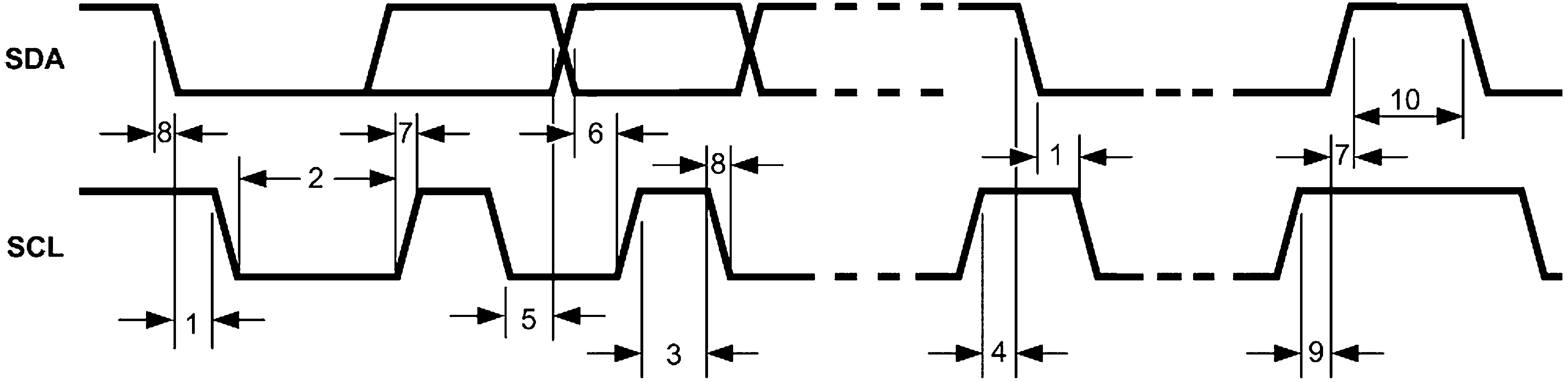 Figure 1. I2C Timing Diagram
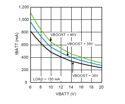
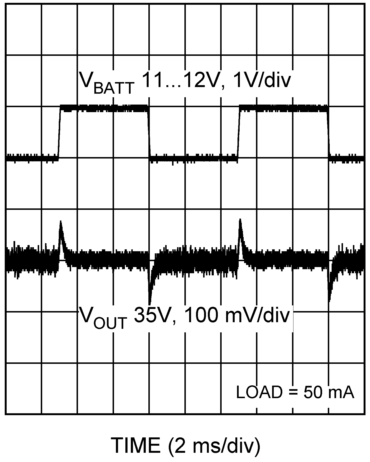
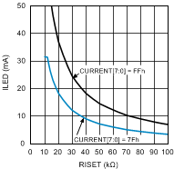
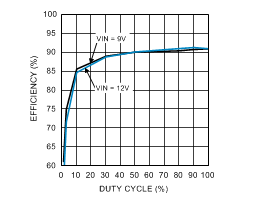
7.12 Typical Characteristics
Unless otherwise specified: VBATT = 12 V, CVLDO = 1 μF, L1 = 33 μH, CIN = 10 μF, COUT = 10 μF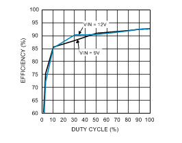
| fLED = 9.6 kHz |
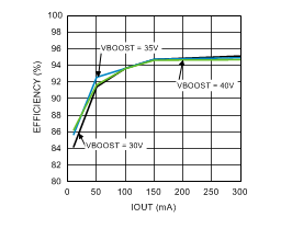
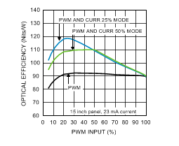
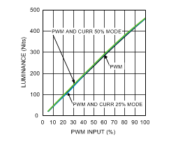
| fLED = 9.6 kHz | L1 = 15 µH |