SNVS159H October 2001 – July 2015 LP3981
PRODUCTION DATA.
- 1 Features
- 2 Applications
- 3 Description
- 4 Revision History
- 5 Pin Configuration and Functions
- 6 Specifications
- 7 Parameter Measurement Information
- 8 Detailed Description
- 9 Application and Implementation
- 10Power Supply Recommendations
- 11Layout
- 12Device and Documentation Support
- 13Mechanical, Packaging, and Orderable Information
9 Application and Implementation
NOTE
Information in the following applications sections is not part of the TI component specification, and TI does not warrant its accuracy or completeness. TI’s customers are responsible for determining suitability of components for their purposes. Customers must validate and test their design implementation to confirm system functionality.
9.1 Application Information
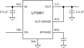
The LP3981 can provide 300-mA output current with 2.5-V to 6-V input. It is stable with a 2.2-μF ceramic output capacitor. An optional external bypass capacitor reduces the output noise without slowing down the load transient response. Typical output noise is 35 µVRMS at frequencies from 10 Hz to 100 kHz. Typical power supply rejection is 60 dB at 1 kHz.
9.2 Typical Application
 Figure 17. LP3981 Typical Application
9.2.1 Design Requirements
Example requirements for typical voltage inverter applications:
Table 1. Design Parameters
| DESIGN PARAMETER | EXAMPLE VALUE |
|---|---|
| Input voltage | 3.5 V, ±10% |
| Output voltage | 2.5 V, ±5% |
| Output current | 300 mA (maximum) |
| RMS noise, 10 Hz to100 kHz | 35 μVRMS |
| PSRR at 1 kHz | 60 dB |
9.2.2 Detailed Design Procedure
9.2.2.1 Power Dissipation and Device Operation
The permissible power dissipation for any package is a measure of the capability of the device to pass heat from the power source, the junctions of the device, to the ultimate heat sink, the ambient environment. Thus, the power dissipation is dependant on the ambient temperature and the thermal resistance across the various interfaces between the die and ambient air.
As stated in the notes for Absolute Maximum Ratings and Recommended Operating Conditions, the allowable power dissipation for the device in a given package can be calculated using Equation 1:

With an RθJA = 56.5°C/W, the device in the WSON package returns a value of 1.77 W with a maximum junction temperature of 125°C and an ambient temperature of 25°C. The device in a VSSOP package returns a figure of 0.565 W (R θJA = 177°C/W).
The actual power dissipation across the device can be represented by Equation 2:

This establishes the relationship between the power dissipation allowed due to thermal considerations, the voltage drop across the device, and the continuous current capability of the device. The device can deliver 300 mA but care must be taken when choosing the continuous current output for the device under the operating load conditions.
The RθJA value is not a characteristic of the package by itself but of the package, the printed circuit board (PCB), and other environmental factors. Equation 2 is only valid when the application configuration matches the EIA/JEDEC JESD51-7 (High-K) configuration in which RθJA was either measured or modeled. Few, if any, user applications conform to the PCB configuration defined by the EIA/JEDEC standards. As a result, the RθJA values are useful only when comparing assorted packages that have been measured or modeled to the EIA/JEDEC standards, but are of little use to estimate real world junction temperatures.
The EIA/JEDEC standard JESD51-2 provides methodologies to estimate the junction temperature from external measurements (ψJB references the temperature at the PCB, and ψJT references the temperature at the top surface of the package) when operating under steady-state power dissipation conditions. These methodologies have been determined to be relatively independent of the PCB attached to the package when compared to the more typical RθJA. Refer to Semiconductor and IC Package Thermal Metrics application report, SPRA953, for specifics.
9.2.2.2 External Capacitors
Like any low-dropout regulator, the LP3981 requires external capacitors for regulator stability. The LP3981 is specifically designed for portable applications requiring minimum board space and smallest components. These capacitors must be correctly selected for good performance.
9.2.2.3 Input Capacitor
An input capacitance of ≊ 2.2 µF is required between the LP3981 input pin and ground (the amount of the capacitance may be increased without limit).
This capacitor must be located a distance of not more than 1 cm from the input pin and returned to a clean analog ground. Any good quality ceramic, tantalum, or film capacitor may be used at the input.
NOTE
Tantalum capacitors can suffer catastrophic failures due to surge current when connected to a low-impedance source of power (like a battery or a very large capacitor). If a tantalum capacitor is used at the input, it must be specified by the manufacturer to have a surge current rating sufficient for the application.
There are no requirements for the ESR on the input capacitor, but tolerance and temperature coefficient must be considered when selecting the capacitor to ensure the capacitance is ≊ 2.2 µF over the entire operating temperature range.
9.2.2.4 Output Capacitor
The LP3981 is designed specifically to work with very small ceramic output capacitors. A ceramic capacitor (dielectric types Z5U, Y5V or X7R) in the 2.2-µF to 22-µF range with 5-mΩ to 500-mΩ ESR is suitable in the LP3981 application circuit.
It is also possible to use tantalum or film capacitors at the output, but these are not as attractive for reasons of size and cost (see Capacitor Characteristics).
The output capacitor must meet the requirement for minimum amount of capacitance and also have an equivalent series resistance (ESR) value which is within a stable range (5 mΩ to 500 mΩ).
9.2.2.5 No-Load Stability
The LP3981 remains stable and in regulation with no external load. This is specially important in CMOS RAM keep-alive applications.
9.2.2.6 Noise Bypass Capacitor
Connecting a 0.033-µF capacitor between the BYPASS pin and ground significantly reduces noise on the regulator output. This capacitor is connected directly to a high impedance node in the bad gap reference circuit. Any significant loading on this node causes a change on the regulated output voltage. For this reason, DC leakage current through this pin must be kept as low as possible for best output voltage accuracy.
The types of capacitors best suited for the noise bypass capacitor are ceramic and film. Hight-quality ceramic capacitors with either NPO or COG dielectric typically have very low leakage. Polypropolene and polycarbonate film capacitors are available in small surface-mount packages and typically have extremely low leakage current.
Unlike many other LDOs, addition of a noise reduction capacitor does not effect the transient response of the device.
9.2.2.7 Capacitor Characteristics
The LP3981 is designed to work with ceramic capacitors on the output to take advantage of the benefits they offer: for capacitance values in the range of 1 µF to 4.7 µF, ceramic capacitors are the smallest, least expensive and have the lowest ESR values (which makes them best for eliminating high frequency noise). The ESR of a typical 1µF ceramic capacitor is in the range of 20 mΩ to 40 mΩ, which easily meets the ESR requirement for stability by the LP3981.
Capacitance of a ceramic capacitor can vary with temperature. Most large value ceramic capacitors (≊ 2.2 µF) are manufactured with Z5U or Y5V temperature characteristics, which results in the capacitance dropping by more than 50% as the temperature goes from 25°C to 85°C.
A better choice for temperature coefficient in a ceramic capacitor is X7R, which holds the capacitance within ±15%.
Tantalum capacitors are less desirable than ceramic for use as output capacitors because they are more expensive when comparing equivalent capacitance and voltage ratings in the 1-µF to 4.7-µF range.
Another important consideration is that tantalum capacitors have higher ESR values than equivalently sized ceramics. This means that while it may be possible to find a tantalum capacitor with an ESR value within the stable range, it would have to be larger in capacitance (which means bigger and more costly) than a ceramic capacitor with the same ESR value. It must also be noted that the ESR of a typical tantalum increases about 2:1 as the temperature goes from 25°C down to −40°C, so some guard band must be allowed.
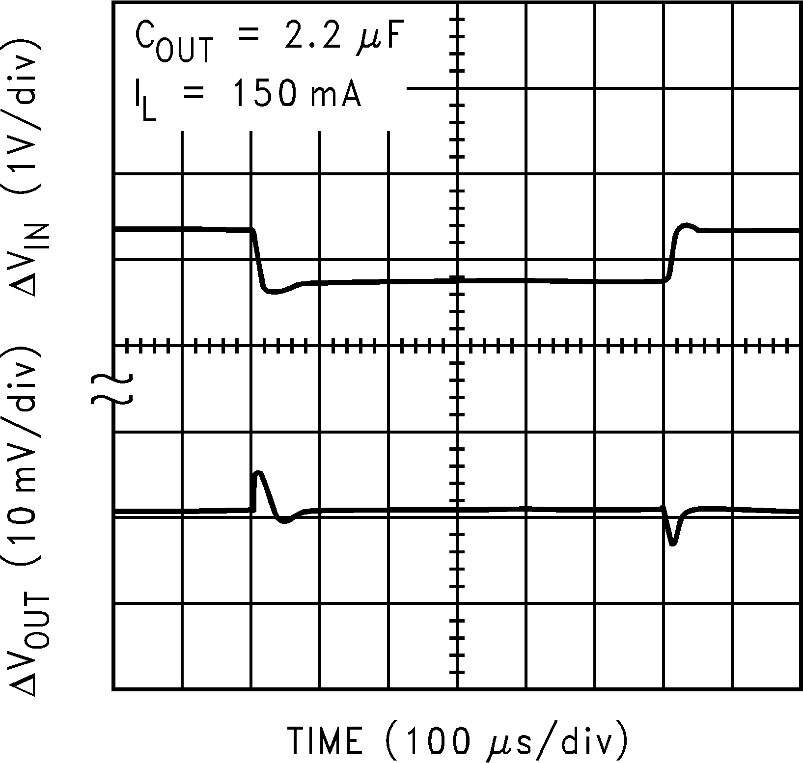
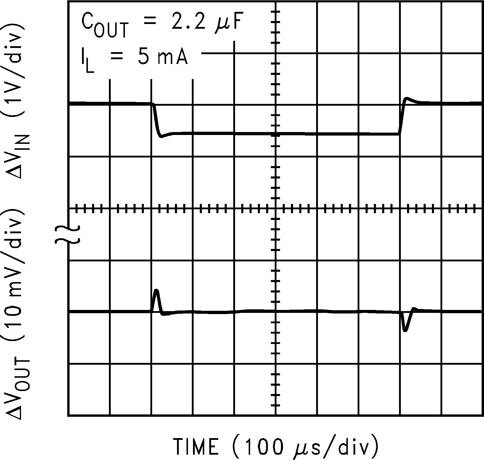
9.2.3 Application Curves

| VIN = VOUT + 1 V to VOUT + 1.6 V |

| VIN = VOUT + 1V to VOUT + 1.6 V |