ZHCSEA3U June 2007 – January 2018 LP3907
PRODUCTION DATA.
- 1 特性
- 2 应用
- 3 说明
- 4 修订历史记录
- 5 器件比较 台式机
- 6 Pin Configuration and Functions
-
7 Specifications
- 7.1 Absolute Maximum Ratings
- 7.2 ESD Ratings
- 7.3 Recommended Operating Conditions (Bucks)
- 7.4 Thermal Information
- 7.5 General Electrical Characteristics
- 7.6 Low Dropout Regulators, LDO1 And LDO2
- 7.7 Buck Converters SW1, SW2
- 7.8 I/O Electrical Characteristics
- 7.9 Power-On Reset (POR) Threshold/Function
- 7.10 I2C Interface Timing Requirements
- 7.11 Typical Characteristics — LDO
- 7.12 Typical Characteristics — Bucks
- 7.13 Typical Characteristics — Buck1
- 7.14 Typical Characteristics — Buck2
- 7.15 Typical Characteristics — Bucks
-
8 Detailed Description
- 8.1 Overview
- 8.2 Functional Block Diagram
- 8.3
Feature Description
- 8.3.1 DC-DC Converters
- 8.3.2
SW1, SW2: Synchronous Step-Down Magnetic DC-DC Converters
- 8.3.2.1 Functional Description
- 8.3.2.2 Circuit Operation Description
- 8.3.2.3 PWM Operation
- 8.3.2.4 Internal Synchronous Rectification
- 8.3.2.5 Current Limiting
- 8.3.2.6 PFM Operation
- 8.3.2.7 SW1, SW2 Operation
- 8.3.2.8 SW1, SW2 Control Registers
- 8.3.2.9 Soft Start
- 8.3.2.10 Low Dropout Operation
- 8.3.2.11 Flexible Power Sequencing of Multiple Power Supplies
- 8.3.2.12 Power-Up Sequencing Using the EN_T Function
- 8.3.3 Flexible Power-On Reset (Power Good with Delay)
- 8.3.4 Undervoltage Lockout
- 8.4 Device Functional Modes
- 8.5 Programming
- 8.6
Register Maps
- 8.6.1
LP3907 Control Registers
- 8.6.1.1 Interrupt Status Register (ISRA) 0x02
- 8.6.1.2 Control 1 Register (SCR1) 0x07
- 8.6.1.3 EN_DLY Preset Delay Sequence After EN_T Assertion
- 8.6.1.4 Buck and LDO Output Voltage Enable Register (BKLDOEN) – 0x10
- 8.6.1.5 Buck and LDO Status Register (BKLDOSR) – 0x11
- 8.6.1.6 Buck Voltage Change Control Register 1 (VCCR) – 0x20
- 8.6.1.7 Buck1 Target Voltage 1 Register (B1TV1) – 0x23
- 8.6.1.8 Buck1 Target Voltage 2 Register (B1TV2) – 0x24
- 8.6.1.9 Buck1 Ramp Control Register (B1RC) - 0x25
- 8.6.1.10 Buck2 Target Voltage 1 Register (B2TV1) – 0x29
- 8.6.1.11 Buck2 Target Voltage 2 Register (B2TV2) – 0x2A
- 8.6.1.12 Buck2 Ramp Control Register (B2RC) - 0x2B
- 8.6.1.13 Buck Function Register (BFCR) – 0x38
- 8.6.1.14 LDO1 Control Register (LDO1VCR) – 0x39
- 8.6.1.15 LDO2 Control Register (LDO2VCR) – 0x3A
- 8.6.1
LP3907 Control Registers
- 9 Application and Implementation
- 10Power Supply Recommendations
- 11Layout
- 12器件和文档支持
- 13机械、封装和可订购信息
封装选项
机械数据 (封装 | 引脚)
散热焊盘机械数据 (封装 | 引脚)
- RTW|24
订购信息
8.6.1.13 Buck Function Register (BFCR) – 0x38
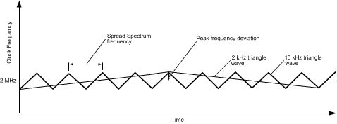
This register allows the Buck switcher clock frequency to be spread across a wider range, allowing for less Electro-magnetic Interference (EMI). The spread spectrum modulation frequency refers to the rate at which the frequency ramps up and down, centered at 2 MHz.
 Figure 44. Spread Spectrum Modulation Frequency
This register also allows dynamic scaling of the nPOR Delay Timing. The LP3907 is equipped with an internal POR circuit which monitors the output voltage levels on the buck regulators, allowing the user to more actively monitor the power status of the chip.
The UVLO feature continuously monitor the raw input supply voltage (VINLDO12) and automatically disables the four voltage regulators whenever this supply voltage is less than 2.8 VDC. This prevents the user from damaging the power source (such as battery), but can be disabled if the user wishes.
Note that if the supply to VDD_M is close to 2.8 V with a heavy load current on the regulators, the chip is in danger of powering down due to UVLO. If the user wishes to keep the chip active under those conditions, enable the Bypass UVLO feature.
| D7-D5 | D4 | D3-D2 | D1 | D0 | |
|---|---|---|---|---|---|
| Name | — | BP_UVLO | TPOR | BK_SLOMOD | BK_SSEN |
| Access | — | R/W | R/w | R/W | R/W |
| Data | Reserved | Bypass UVLO monitoring
0 - Allow UVLO 1 - Disable UVLO |
nPOR Delay Timing
00 - 50 µs 01 - 50 ms 10 - 100 ms 11 - 200 ms |
Buck Spread Spectrum Modulation
0 – 10 kHz triangular wave 1 – 2 kHz triangular wave |
Spread Spectrum Function Output
0 – Disabled 1 – Enabled |
| Reset | 000 | Factory-Programmed Default | 01 | 1 | 0 |